-
AI and the intelligent Factory
I recently watched Jeff Winters keynote from the 2026 PROVE IT conference
The Intelligent Factory: Why Manufacturing Needs a New Operating ModelIt extremely well sums up 2 things:
1. a super compressed overview on AI history and how AI works
2. what are the possibilities if used in manufacturing – with the right approachBelow is the link to the complete keynote on YouTube (~57 minutes) as well as the slide deck Jeff showed.
There is plenty of more excellent Industry 4.0 content on Jeff’s homepage:
https://www.jeffwinterinsights.comThank you Jeff for this outstanding keynote talk.
-
Humanoids in Wafer FABs – update
I was curious what the world of AI thinks 2 months after the initial poll and gave the same chatbots the exact same prompt like I did in early January.
To my big surprise the picture changed indeed – significantly !
Below is the comparison of the 2 response to the prompt:
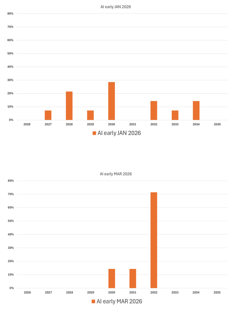
It is very interesting to see, that almost all models now come to the same conclusions and I wonder is this because of they all use now more and more the same underlying data or is the underlying data itself no more “precise” and points towards a 2032 date.
Another interesting fact was that most models mentioned in their response, that
-
Legacy FAB Automation Maturity – Update
I like to share the latest update of the SEMI effort regarding legacy FAB Automation Maturity.
Dennis Xenos from Flexciton presented last week at the Innovation Forum in Dresden, Germany the latest results – there is now data from 9 FABs available:
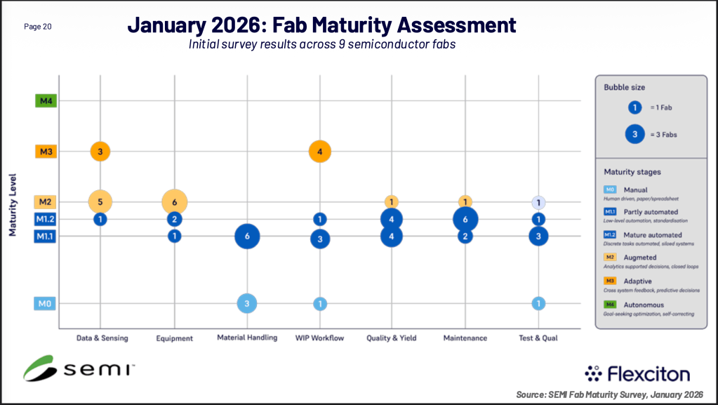
The complete presentation can be found below:
The team is still looking for more FABs and industry experts to participate – if you have interest in joining the effort please reach out to
Anshu Bahadur, email: abahadur@semi.org
-
Humanoids in Wafer FABs – poll results
First of all I like to say thank you for the active participation. As we just saw at CES – humanoids are “really everywhere” – but it also seems there is a long way to go to see these comrades in real productive deployments.
Here is the poll result:
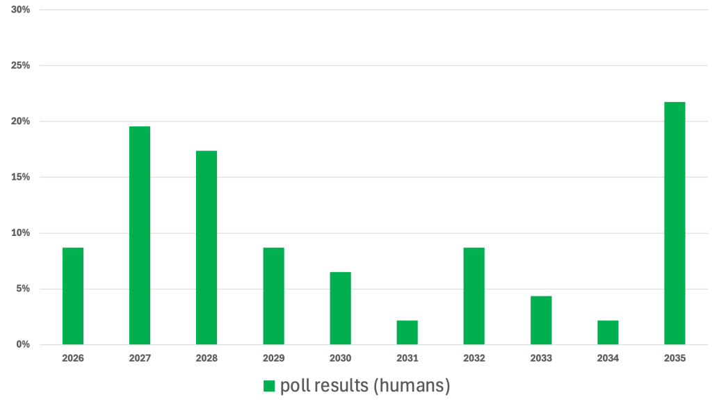
Based on this data about 50% of the voters expect deployment within the next 3 years, but there is also a large fraction which points to a much later date.
I was curious what ChatGPT & Co. think about this topic and asked a bunch of different AI tools and also did this within 3 weeks twice – and yes, the same AI app changed sometimes the expected deployment date between the 2 inquiries by up to 2 years.
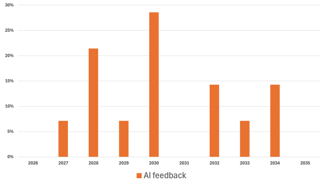
A cumulative chart comparing the two results shows this:
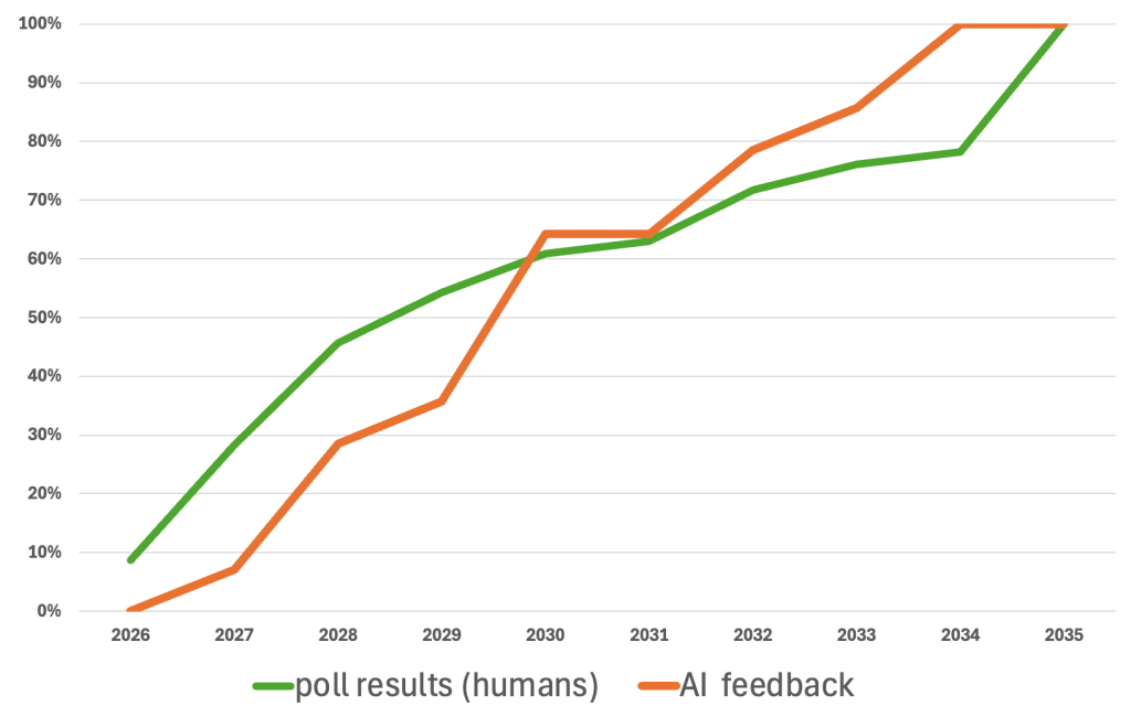
The AI feedback was generated by using this prompt:
“I like you to act as a technical researcher and planner. In which year will we see the first humanoid robots working in regular production in semiconductor frontend wafer fabs. Please list the top 3 facts you have used for your estimated year and back it up with data. Please tell me the year, when you have 80% confidence that the humanoid robots are deployed – not in test mode, but in normal production, executing wafer carrier transport as well as process tool loading and unloading fully autonomously. I’m only interested in your estimated year for fabs in the US or Europe, not in Asia”
This prompt does not only deliver a simple date, but a few interesting statements and remarks about the what and how of the deployments – give it a try yourself !
When it will really happen – only the future will tell us – but one thing is sure: If your company wants to be a front runner for this effort the start of the work on how to integrate humanoids into the Wafer FAB software ecosystems needs to happen very soon.
Lastly, I ran into a nice video talking about humanoids in homes – which I think is an even more complicated deployment – worth watching.
So with all this – when do I think we will see a humanoid in a wafer FAB ? Being a technical optimist I say it will be sometime in 2028 – 2029.
Thank you for following and reading my blog.
2 responses to “Humanoids in Wafer FABs – poll results”
-
A thought:
Why does the world need humanoid robots? My bold hypothesis: it doesn’t need them at all. At least not for technical reasons. Perhaps for psychological reasons: for example, if robots work with people in need of care, it would be helpful if they could speak and move like humans. But in a factory? There are better automation solutions than imitating humans. Do you know how complicated it is to replicate just a human hand? Let’s abandon this delusion. In a factory, we need solutions. They can look like humans, but they don’t have to.Translated with DeepL.com (free version)
LikeLike
-
-
Humanoid Robots in Wafer FABs ?
As the activity and hype (?) around humanoids heats up there is one question lately in my mind: When will we see the first humanoid robots in wafer FABs in regular production ?

Since the overall trend towards more generic robotic hardware is gaining traction the human form factor will fit of course very well in all older wafer FABs which have no OHT capable automation systems – largely because of too low ceilings and recessed equipment load ports. In todays application often AGV/AMR solutions are deployed, but as humanoids will eventually become commercially available.
Obviously there is still some significant work to be done especially for topics like:
- physical safety ( what happens if a robot falls)
- working in hybrid environments with real humans
- gripper capability / flexibility
- run times per charge
- how long will it take to train and commission and humanoid
To have generic humanoid robots which will be able to work the next day in a different FAB area – just by a software change – would be the ultimate benefit.
I also think there will be some work needed to integrate humanoid robots into the typical FAB software environment:
- will they be controlled by a traditional MCS or fleet manager ?
- will humanoid robots “speak” SECS/GEM and E84 ?
Besides all these challenges I believe humanoids will find there way into the wafer FAB automation world: be it
– to transport wafer carriers
– load / unload process tools
– transport spare parts to support maintenance crews
– execute the complete maintenance work from start to finish.I’m curious what you – the reader of this blog – think. By when will we see the first humanoid robots doing regular production work in a wafer FAB in the US or Europe ? Please participate in the poll below.
I will share the results next year in my next post.
Happy Hollidays !

-
Maintenance in the era of Industry 4.0
I recently run into a very nice article written by Jeff Winter – discussing the evolution of maintenance approaches. I thought it is absolutely worth sharing here.
Thank you Jeff for giving me permission to do so. More interesting articles by Jeff can be found here:
https://www.jeffwinterinsights.com/Please see the article here:
-
Legacy FAB Automation Maturity Framework
In the last 3 months there was a working group under the umbrella of SEMI working on a Maturity Framework – and the 1st results were presented at the SemiCon West last week in Phoenix, AZ.
I had the opportunity to contribute to this work. The attempt is to give existing 200mm Wafer FABs an idea where they rank in terms of automation and autonomy – and eventually a guide where to start with the efforts to catch up.
With the increasing pressure from chips made in Asia – especially legacy nodes technology based – there is only one way to stay competitive: get more output out of the existing factory – ideally with less cost.
Automation and eventually Autonomy using advanced algorithms ( I did not say AI !) will definitely be the way.
Below you can find the presented slides:
As always, the more FABs participate, the better will be the outcome and quality of the frame work. If you are interested to participate – see contact information on the last slide of the attached file.
-
Results of FAB Automation 2025 survey
I like to thank everybody who participated in the survey in the recent weeks. The survey had 5 different focus areas:
– 100/150mm Frontend FABs
– 200mm Frontend FABs
– 300mm Frontend Fabs
– Assembly/Test/Backend
– non semiconductor hight tech FABsUnfortunately, only the 200mm Frontend section got enough participation to assume that the results are statistically relevant. Not sure how to explain the “silence” of the other areas – maybe automation is not a hot topic there at all.
Nevertheless, I think the results for the 200mm Frontend FABs are very interesting and to some part surprising.
I would love to hear your thoughts about the results in the comment section of this post !
The survey results can be found here:
Leave a comment
-
State of Semiconductor FAB automation in 2025
In a recent discussion with my colleague Wesley Capar – talking about FAB automation and what the overall situation in the current difficult business environment might be – we came up with the idea to ask YOU – the industry experts on your opinion.
Since the situation is likely very different between state of the art 300mm FABs and older legacy facilities, I structured the survey in 5 individual parts. The questions itself are 100% identical in each survey – the only difference is for which facility type your answers are coming from:
- 200mm Frontend FABs
- 15mm/100mm Frontend FABs
- 300mm Frontend FABs
- Assembly/Test/Backend FABs
- other high tech / clean rooms FABs
The results of the surveys will be posted once they are in.
Thank you for reading and participating – it will take less than 10 minutes of your time.
Below are the 5 surveys:
Please use this survey if you are answering for a 200mm Frontend FAB:
Please use this survey if you are answering for a 150mm/100mm Frontend FAB:
Please use this survey if you are answering for a Assembly/Test/Backend FAB:
Please use this survey if you are answering for a 300mm Frontend FAB:
Please use this survey if you are answering for other high tech / clean room factories:
-
Importance of carrier location tracking – part 2
This post will be all about the advantages and capabilities of RFID based carrier tracking.
But before I dive into this – here are the results from the poll from part 1:
Based on this more than half of the legacy FABs have no complete location tracking of all carries in place. In my opinion this is not surprising. A main reason for this situation is that all these FABs are running production for many years and have found work arounds to limit the impact of the missing exact location tracking. A great part of these work around processes play humans – who are able to search and locate carriers. Of course this comes at the cost of spending the time for searching – which reduces FAB productivity.
As competition increases and the ever ongoing fight for reducing the cost per wafer in the FABs leads FAB managers to start thinking about automating material transport and handling – exact location tracking becomes a must. As discussed in part 1 of this blog there are various methods to achieve this, but the quasi industry standard is using RFID.
How does RFID work ?
Every carrier to be tracked needs to have some form of a RFID pill or RFID tag attached to it. This tag holds information about the tracked carrier, for example the carrier ID. In order to locate a carrier every place where a carrier can be placed needs to have an RFID Antenna which can detect and read the RFID tag information.
There is a fundamental important (and kind of hidden) meaning in this statement:
every place where a carrier can be placed needs to have a RFID AntennaFor true 100% location tracking no carrier is allowed to be placed somewhere without a RFID antenna. (classic examples for this could be shift leader tables, WIP overflow shelves, …)
When introducing RFID based carrier tracking a lot of existing FAB policies will need to change – but more on that later.
Here is a picture about the general infrastructure needed:


There are different frequencies for RFID system available on the market:
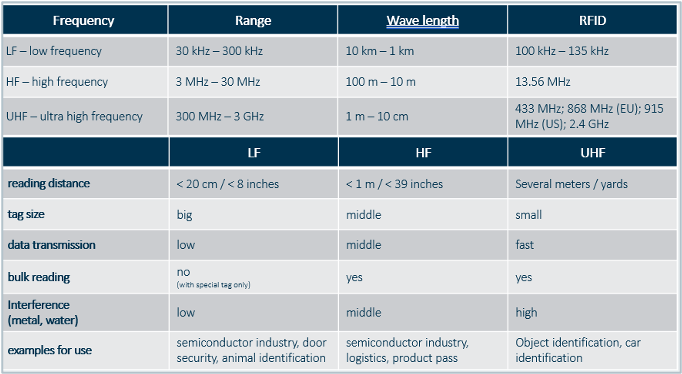
All of them have their individual strengths and weaknesses, but in the semiconductor industry the low frequency or LF is the quasi standard. Greater 95% of all FABs which use RFID based carrier location tracking use LF – biggest reasons for using LF are:
- very short reading distance (avoids cross reading of multiple RFID tags , for example in shelves or nearby load ports
- very narrow bandwidth ( helps in the general high radio frequency noise inside the FABs)
- plenty of different antennas available to accommodate antennas to be placed in difficult physical locations (like tight load ports)
Like already discussed in part 1 of this post there are many benefits of having good location tracking in place:
- no more time lost for searching carriers (lots)
- effective FAB scheduling is possible
- basic enabler for automatic material transport and handling
- basic enabler for automated process start on equipments
What makes RFID based material tracking the better choice over bar code scanning based solutions are things like
- highly reliable (not dependent on good lighting)
- many tool load ports come standard with RFID reading capabilities or can be easily upgraded
- no human interaction needed (hand scanning) – massive time savings possible
A few thoughts on how to approach an project to change a FAB to RFIDIntroducing or changing carrier tracking methods are a complex task since a lot of existing policies might change. Change in itself always brings some risk with it and if it is involving possible productivity and/or wafer loss – sensitivity is extra high. Since every FAB has some form of carrier identification and location management in place (see part 1 of the post) the desire for change and improvement typically comes from cost pressure – either reduction in operator cost and/or growing plans to automate carrier transport, handling and decision making
A fundamental decision to be made at the very beginning of such a project is:
What is the end goal – in 5 or 10 years ?What is the expected automation level of the FAB in 10 years from now ? Will the FAB always have operators or is the plan to have eventually 100% automation of “everything” ?
The statement:
every place, where a carrier can be placed needs to have a RFID Antenna
often raises fears on the overall cost of such a project.But at a second look there is seldom a big bang event possible, where “overnight” everything has to be changed and in place. One big advantage of RFID based ID and location tracking is: It can be easily implemented in phases. In other words, there can be a long lasting hybrid approach used. Some areas start using RFID other keep doing what they do today. There might be even cases in older legacy FABs where not all locations and equipment load ports can be outfitted with the needed RFID hardware – but why not harvesting the benefits on 85% of all the others ?
The only true initial cost is that all to be tracked carriers need to have an RFID pill or tag attached to it.
What will it cost ?
Let’s assume the FAB has 6000 carriers (cassettes for example).
Depending on the RFID tag or RFID pill vendor, the cost should be around $10 or so. So we are talking $60,000 for the whole FAB.
In addition, there might be cost on how to attach the pill or tag to the carrier. This depends on what is already available at the existing carrier. In the best case there is zero additional cost (pill or tag holder already existing) or there will be very manageable additional cost to weld holders on the carrier.
The bigger cost driver is the actual roll out of the RFID antenna / reader / Ethernet connection boxes. The good thing is, it can be rolled out very step by step. For example: to start with RFID antennas for a certain tool group, just the RFID reader hardware needs to be procured and installed on these tools. This is anyway a recommended great 1st step to iron out any possible integration efforts with the local FABs MES system. Once this is working – maybe even including “load and forget” scenarios to automate process starts on the selected process equipment – further roll out can be planned better.
Using this approach the total project cost can be distributed over years if desired and the most beneficial tool sets (high operator effort for example) could go first …
Final Thoughts
For existing legacy FABs with aged process and metrology equipment one key aspect of such a project is to make sure that all desired equipment can be upgraded with reliably working RFID reading hardware.
I strongly recommend to partner with an RFID expert like (spoiler) FABMATICS (LINK) to test in your FAB at your specific equipment which antenna and reader combination works best for each tool type, shelf or buffer location- at the lowest possible cost – basically mounting RFID tags and antennas in various positions with actual carriers.
If you are early in your project and still free in decision making, here is my general recommendation:
- partner with an experienced RFID Semiconductor FAB retrofit company, not only for hardware and software, but also for the general concepts ( for example should you use re-writable tags or not as well as what capability you MES can provide)
- go with LF RFID solutions – if possible with pills
- plan for complete full automation in the future, to make sure your RFID infrastructure selection can support this longterm (number of different antenna types possibly needed) as well as AMHS and robotic systems which support RFID based ID tracking (way more reliable than bar code)
- plan to start with a pilot tool set
- run this pilot in production for some time and learn
- roll out tool group by tool group
-
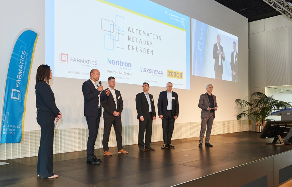
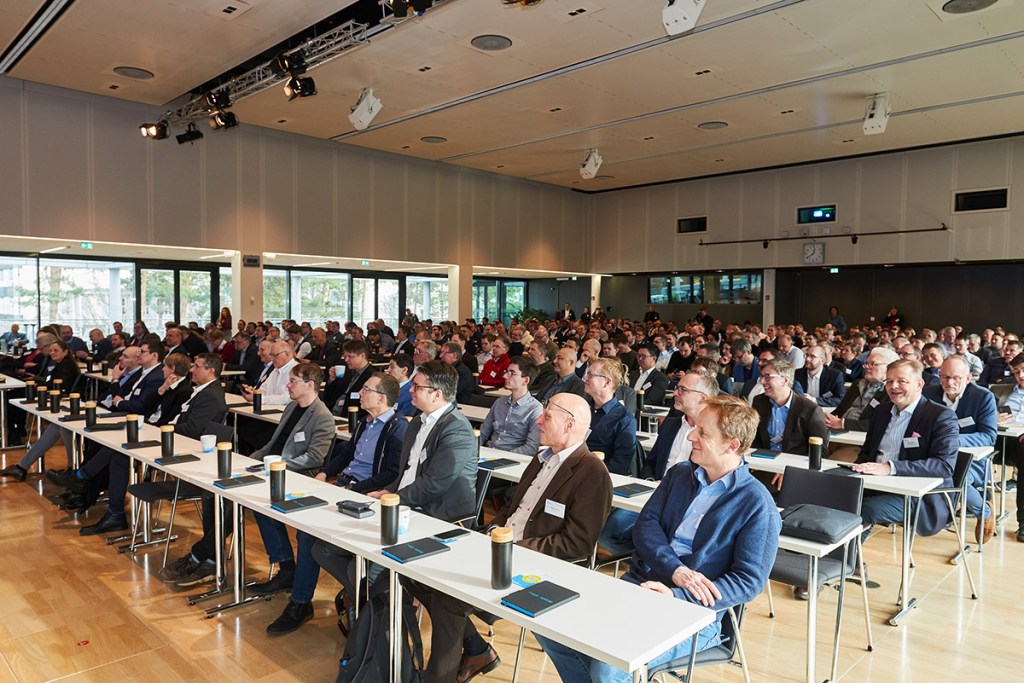
Innovation Forum for Automation 2025
To make it short: We had a blast !
The 22nd edition of the conference took place in Dresden, Germany last week and I had the honor to play an active part. Together with a few of my colleagues from Fabmatics Germany we hosted the break out session
Test Wafers – the hidden GEMS in your FAB

It was a packed room and all three presentations stimulated a very active Q&A session which clearly showed that the topic is still hot in the industry. This was the session layout:
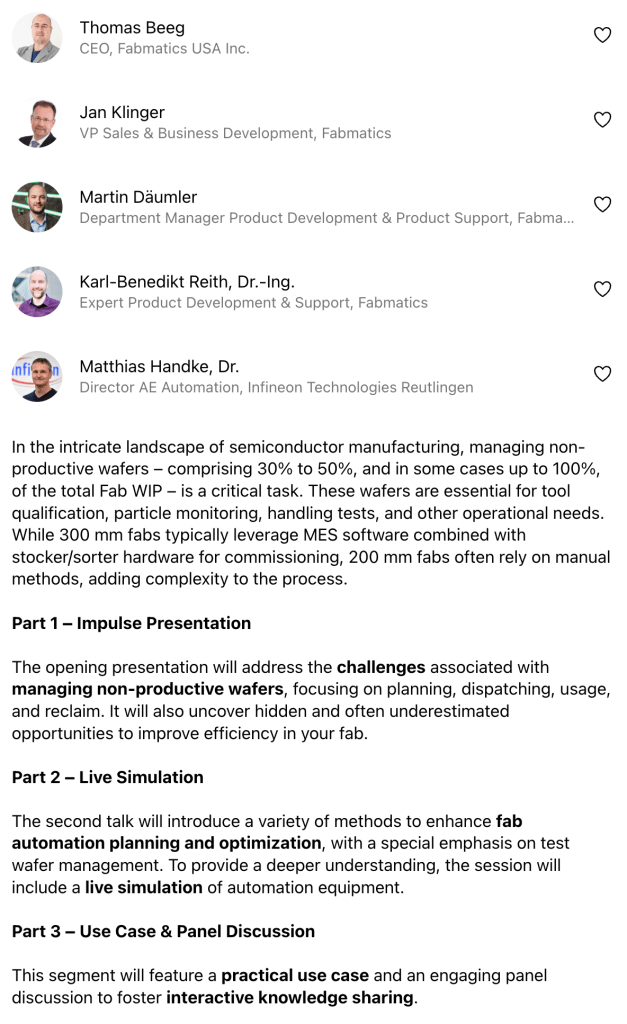
here you can find all 3 slide decks:
On day 2 of the event I had the opportunity to participate in an expert panel to discuss hot topics of the semiconductor industry – specifically for the none-leading edge eco system.

On both days plenty of interesting talks were given – but one was especially eyebrow raising in my mind:
Dr. Matthias Meyer from the Fraunhofer-Institute talked about soon to be established regulations for cyber security in the European market space. If you are active there – please have a look here:
Finally, a few impressions from the event – a big thank you to Automation Network Dresden/Photographer: Sven Claus, who was providing the pictures for this post.


-
Good Bye 2024 – Hello 2025 !
Another super busy year went by like a breeze – and I like to wish all my readers a great Holiday Season and a good start into 2025.
Speaking of 2025 – there will be 2 great conferences early next year which I plan to attend and I like to raise your interest.
Innovation Forum for Automation in Dresden, Germany

The agenda was just published and there will be again great topics to listen and learn from:
AGENDAI will be an active participant this time – talking with some of my peers from Fabmatics about

Advanced Semiconductor Manufacturing Conference – ASMC in Albany, NY

As a member of the Technical Committee of the ASMC I just participated in the conference prep meeting and we put together a great selection of presentations and posters. The final agenda has not been published yet – be sure to check the ASMC website in the next weeks.
Maybe you will be at one of these 2 events, too – looking forward to meet in person.
Until than – Happy Holidays !
Thomas
-
AI enabled precision maintenance
I’m very happy to have another guest post to publish ! During the last SEMI Fab Owners Alliance (FOA) meeting in Portland, ME
David Meyer, co-founder and CEO at Lynceus AI and
Ariel Meyuhas, COO and Founding Partner at MAX Grouppresented a very interesting approach using AI to improve equipment maintenance. I think this is a really nice approach to tackle a long existing problem in the industry. I approached David and Ariel to share there work here – Enjoy reading !
AI-enabled Precision Maintenance
This blogpost follows a presentation made at SEMI FOA session in October 2024. The slides are attached below.
AI-Enabled Precision Maintenance: a new way of managing capital capital equipment
As you all know, servicing tools becomes increasingly complex and PM checklists keep growing. If we keep thinking about maintenance in the same way, we risk degrading COO and profitability. On the brighter side, there is now abundant data to describe equipment behaviour and the technologies that can leverage this data are getting more and more mature.
This is an opportunity to provide a step-change in equipment productivity.
Current Maintenance Paradigm: long, rigid and blind
Here is the problem: we are used to fixed PM schedules. At every PM, we run through the same list of actions – irrespective of what’s actually happening to the tool / process.
As a consequence, our PMs are long, rigid and blind.
This negatively impacts PM downtime, qual complexity, spare parts consumption and even unplanned downtime. The time we spend on unnecessary interventions is time we could have spent troubleshooting more accurately or implementing longer term fixes.
Now, what if we could run PMs differently? what if we could do only what is necessary, when it is necessary?
This is what AI-enabled Precision Maintenance aims for.
A new maintenance concept
We came up with the concept of a dynamic and fractional PM checklist based on real-time status of the tool and of the process. Concretely, for each part of the tool and at any given time, we can recommend whether or not an intervention is required.
We formulate this recommendation based the tool’s maintenance history and on its most recent behaviour.
With AI-enabled precision maintenance, you’d be able to access real-time recommendations, for each part of the scope: how many wafers can I still produce before change? is the tool behaving normally or not?
This tool has the power to optimize PM scheduling and inform the engineer on which parts of the PM scope to execute or not.
This translates into:
- Shorter G2G
- Simpler PM, and therefore simpler quals
- Reduced spare parts consumption
- Improved team productivity
As a fab manager, it gives you the possibility to optimize for COO, productivity and capacity simultaneously. The concept was tested on a bottleneck toolset with manual extraction of data, which is very labour intensive.
Combining expertise
Rolling-out AI-enabled precision Maintenance successfully requires a combination of different skills & expertise working together.
First, deep Maintenance & Equipment expertise: MAX Ops defined the Precision Maintenance concept and demonstrated its impact through manual implementation. We know it works, but it is still more empirical than systematic.
Then, we need to make it scalable. AI techniques help extract and leverage information from equipment data automatically, which then feed dynamic PM checklists.
The last piece of this puzzle is of course the users in the fab. Adopting such a novel approach to capital equipment management requires a true partnership with the fab, in order to define the best way to validate, deploy and use this tool.
Impact on Operations
While AI-enabled precision maintenance is a new concept, Precision Maintenance is not.
At MAX Engineering, we have been supporting fabs in optimizing their maintenance cycles by defining more frequent, more fractional scopes – with some great results.
In this example, we were working on a set of Litho tools in a 300mm fab.
Precision maintenance helped this fab reduce G2G time by 25% on average and improve M-Ratio from 3 to 5:1. On an annualized basis, this means 4% net uptime gains.
Now this is what you can obtain by breaking down PMs into smaller fixed scopes, through a highly manual and empirical process.
So what is the expected impact of boosting Precision Maintenance with AI?
First, we would be able to define dynamic PM scopes, updated in real-time based on the tool’s most recent behaviour. We expect this can double the productivity gains evidenced with Precision Maintenance, parts & people combined.
Second, we could replicate this approach seamlessly to other bottleneck areas in the fab, 6 times faster than if we had to redo it manually. At scale, this means turning local uptime gains into realized throughput expansion.
Looking forward: AI-Module Engineer Assistant
To conclude, I’d like to give you an idea of what the future of module engineering can look like.
We saw that AI-Enabled Precision Maintenance will be a step change in maintenance productivity, but this is only step 1.
We are already working on an AI module engineer assistant, able to perform most of the routine tasks around process & equipment management. We imagine a tool that can:
- Flag drifts in equipment behaviour
- Define maintenance checklists based on the tool’s most recent behaviour
- Publish and share reports on recent PMs
- Build correlation studies around events of interest
- Support technicians during interventions
This is step 2, and we’re working on it today.
Here is the complete presentation from the SEMI FOA meeting:
If you are interested to learn more, please contact David or Ariel directly:
David Meyer : david.meyer@lynceus.ai
Ariel Meyuhas : ariel_meyuhas@maxieg.com -
Importance of carrier location tracking – part 1
When looking on the topic of improving Wafer FAB performance – the topic of lot and/or carrier tracking is often not in focus. For fully automated 300mm FABs this is really not an issue, because it is fully covered using RFID tags/pills on the FOUP and have any possible place where a FOUP can “sit” outfitted with RFID antennas. This ensures that at all times the exact location of a FOUP (and the associated lots) is known.
For legacy FABs running 200mm or 150mm the topic of carrier and lot location is far from being standardized and solved.
Why is it important ?
In Lehmans terms: if the location of a carrier (and the lot or lots) is not exactly known, it might create wait time and lost tool utilization since “someone” needs to “search” for it. These little search times can easily add up and become a problem. If a FAB wants to go from a more manual material transport and handling to a more automated solution the topic becomes very critical.
But even in manual FABs the real time knowledge of the current location of a carrier can have big impact.
A typical use case is to move from pure lot dispatching towards lot scheduling to improve the overall FAB cycle time and tool utilization. Without exact lot location a schedule is “worthless” since the schedule can not be executed. Because the lot is not available when needed. I have in person witnessed legacy factories which had scheduler deployed, but more than 10% of the WIP’s location was not known and therefore the schedule could not be executed. Typically the quality of the scheduler solution gets questioned , but the real problem is the unclear lot location data situation.
Let’s explore the situation – specifically for not fully automated factories
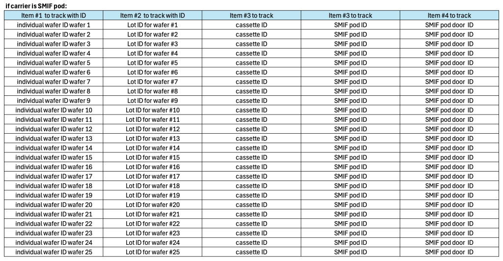
The first interesting thing to discuss is the lot and carrier identification itself. Depending on the used carrier in the FAB the complexity is different. The tables below show the theoretical depths of the problem:


For practical reasons not all of the items might be tracked in the real FAB application.
How are the individual parts ID’ed ?
There are different methods used for different parts.
Wafer identification
Individual wafers are typically tracked by using a physically laser scribed ID number directly on the wafer. This means the ID is fix for the lifetime of the wafer – it cannot really be deleted and given a new ID.
A lot ID is not a physical thing, which can be location tracked since a lot ID is a virtual entity residing in the MES. Multiple individual wafers (and their ID number in the MES) are logically grouped and called a “lot”. Common approach is that all wafers of one lot have the same target product and will be put in the same carrier. The mapping of wafer ID to lot ID traditionally happens at lot start in the FAB and will be stored and tracked in the MES.
Cassette identification
In the early days cassettes were ID’ed by putting labels with a form of code – typically bar code – on it. Additionally to the bar code there is often a human readable number on the label. To locate a cassette for example in a WIP rack, a human would scan with his/her eyes the rack until the cassette is found.
Example:
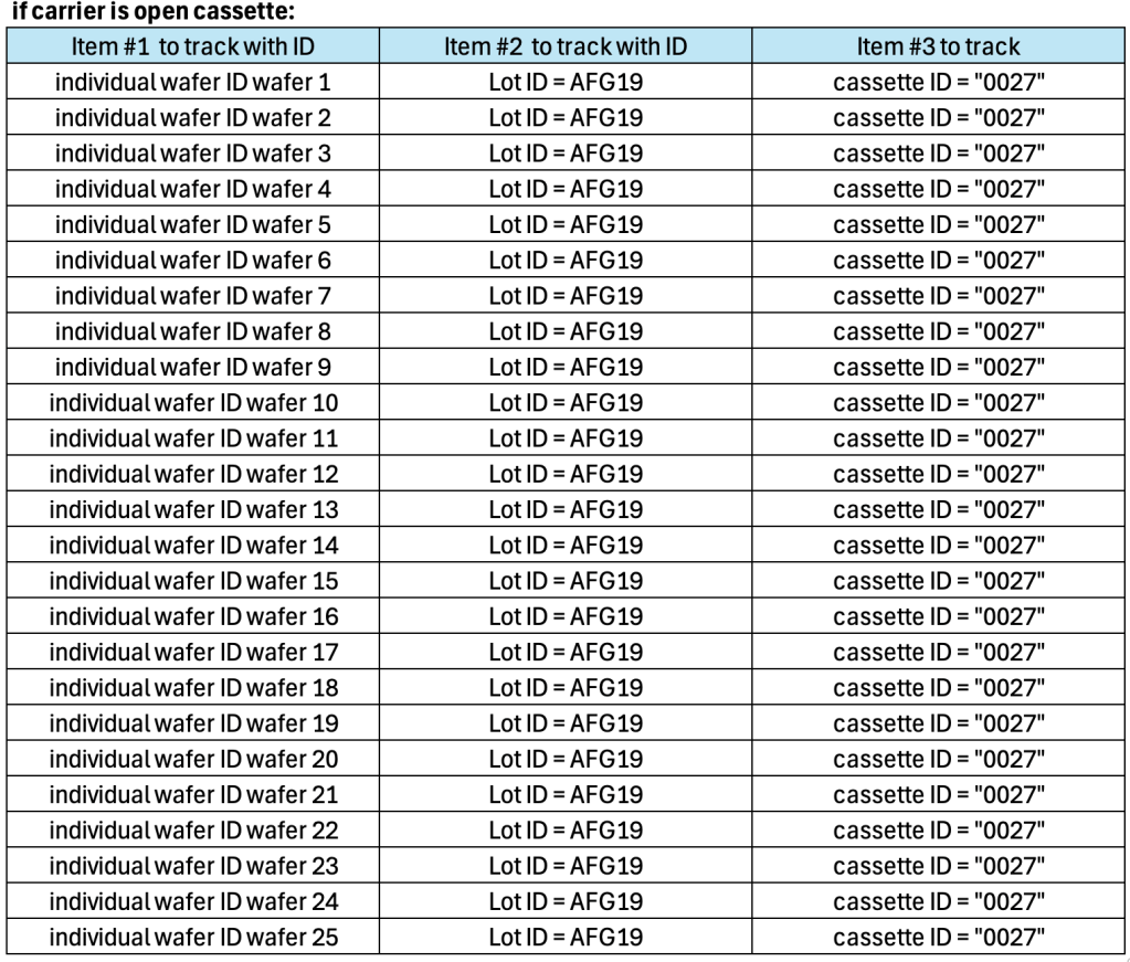
In the example above only 2 ID would be visible to humans or machines on the physical cassette: the cassette ID and if looked very close, the individual wafer IDs. The lot ID is usually not visible on the cassette, unless an additional lot ID label is recreated and attached to the cassette.
Therefore humans in the FAB often look for the visible carrier ID when searching for “a lot” but not really for the lot ID.
Using barcodes on the cassettes brought the advantage to use bar code scanners for data entry into the MES and therefore eliminating possible human errors while manually entering awkward lot and carrier ID into a computer terminal. Downside of the label with code method is that there are physical code scanner devices needed – many of them. In the real FAB 24/7 often these scanners create problems, especially if they are wireless and have rechargeable batteries. Network stability in fully packed legacy factories is often a challenge and battery life as well is “where is the scanner ?” create additional risk for lot processing delays.
A second – way more capable method of ID-ing cassettes – is the usage of RFID tags or pills. These pills can hold multiple sets of information and can easily be re-programmed with new content. The possibilities and advantages of RFID based carrier identification and location tracking will be topic of part 2 of this post.
Lot box identification
If a FAB uses cassettes in a box another element for tracking comes into play,. Should the box be tracked with an ID for the box itself on top of the cassette ID ? In my opinion the answer is yes. There are many advantages of doing so:
- boxes and cassettes might be restricted for usage only in certain zones (FEOL, BEOL, Copper , …)
- in a manual FAB, the box is what humans will see in most cases (since the cassette is inside)
- when cassettes are loaded onto an equipment load port the empty box needs to be stored “somewhere”. In many cases the same box should be used again once the cassette is done with processing
- there are steps in the process flow, when wafers need to be moved from the transport cassette into a special processing cassette – without ID it will be a risk to mix ups
- in case of equipment break down during process wafers from multiple lots, cassettes and boxes might need manual recovery – huge potential of mix ups, if proper IDs are missing
One typical question which needs to be answered when setting up cassette and box ID is: How is the relationship between the 2 defined.
For example:
At lot start a brand new cassette and brand new box will get for the 1st time an ID label, lets assume
Cassette ID = WC0028 and the Box ID = WB0028
Wafer ID will be assigned to a lot ID and after that the wafers get physically moved into the cassette and the cassette into the box. What will be the FAB policy regarding to the cassette to Box relation ?
Option 1: WC0028 always needs to be in WB0028
Option 2: there is no hard requirement for following Option 1 always, WC0028 can be for example transported in WB0017, as long as such a change is tracked within the MESBoth cases have their pros and cons, but in my experience option 2 is the most used one.
There are also cases where the box itself is transparent or has a transparent window and the cassette ID can be read by humans through the box. In these rare cases sometimes the box is not tracked with an own ID – with all the downsides of that.
SMIF Pod identification
SMIF pods introduce a 3rd part which could be tracked since the “lot box” now is a Pod which has 2 individual physical parts – the dome and the door. In general all statements from the section lot box identification can be made for SMIF Pod as well. The most interesting question for SMIF Pods is:
Is there value in tracking dome and door individually ? The answer depends a lot on 2 things:
1. Has the MES the capability to easily track additional objects ?
2. Does the process provide contamination risk, if the wrong door gets put on a dome ?
Now that the basic principles of the identification of carriers are discussed, let’s look into the location tracking aspect. In general location tracking for my purposes here mean:
“to know, where a specific carrier (carrier ID) is right now in the FAB”
There are 2 sub topics here: “Where” and “right now”
“Right now” is a simple correlation to date and time. If this data is available and stored in a computer system, then also the historical positions of a carrier can be looked up. The more interesting part is the “where”.
Although there are tracking systems available, which track “indoor GPS style” using X, Y and Z coordinates, it is more common to have defined places as the “location”, examples:
- Stocker 17 in bay 5
- incoming WIP ETCH bay rack 1
- load port 2 at equipment ID ETC003
- shift supervisor desk in main aisle
- on cart 3 of intra-bay transport system
- WIP rack 22, position 6
- push cart 4 (on the way to Litho area)
All these “locations” have some context related information and humans will remember, where WIP rack 22 is physically located. The interesting aspect here is, that humans are capable to use relatively “vague” locations like “it is in WIP rack 17” to hopefully quickly find the specific carrier – by browsing the carrier rows and look for the carrier ID.
How is the “carrier ID to location” relationship established and available for users (humans or machines) ?
There needs to be some form of track in / track out mechanism into a specific loaction.
for example:
- when a carrier is placed into a rack , the carrier ID as well as the rack id get bar code scanned
- when a carrier is placed on an equipment load port, the carrier ID and the load port ID get bar code scanned
- when a carrier is placed on a WIP Rack, the location is manually entered in a MES terminal
- or in its simplest form, without any tracking: “all incoming WIP to this bay gets placed in to the “incoming WIP rack”
The quality of the location data and its resolution can have a big impact:
” it is in rack 17″ might be good enough for a human, but if there are plans to automate material transport “it is in rack 17” will be a hard showstopper or at least very time consuming for a robot to scan all possible individual rack locations.
In general it can be said, the better the location data resolution is, the faster a carrier can be “found”.
In fully automated 300mm FABs any possible location a carrier can be in is individually specified and has an individual location ID. These are used by the MES and MCS system. For legacy factories with 150mmm oder 200mm wafers this location resolution is much more coarse.
I’m curious what nowadays the typical location data quality is. If you have knowledge about this topic in 150mm and 200mm FABs ( please no 300mm data ) please answer the poll below:
I will share the results in part 2 of this post.
Thank you for reading.
-
Test Wafer, part 3
In the last few weeks I had the opportunity to visit a few of our (FABMATICS) customer FAB’s here in the US – sure enough the topic of test wafers and the options and benefits to automate test wafer handling came up in all of them.
They all categorized themselves into the area of higher test wafer to product wafer ratios ( see the 1st post of the test wafer series) and mentioned they feel they have way to many test wafers in the FAB. Most of them also talked about challenges in getting tool time on process equipments to build new or recycle used test wafers.
From my own experience this is very common in less automated FAB’s where a lot of day to day decisions are still made by humans – who are often measured by daily or hourly production wafer moves.
To get a good control over the huge number of test wafers and the high number of different test wafer products one key starting point is to have transparency about test wafer WIP levels, use rates and who owns which test wafer.
I think to have a chance to be successful the general FAB mindset needs to be that test wafers have the same importance as production or engineering wafers.
This means that test wafers are completely modeled and tracked in the FAB’s MES system and test wafer lots are “running” on test wafer routes or flows – exactly like production wafers. This will not only enable real time monitoring of the test wafer status, but also opens up the capability to schedule and dispatch test wafers automatically using the FAB’s scheduling systems.
Test wafer Modeling
There are many ways of modeling test wafers, but one successful way of doing this is to follow the general life cycle of test wafers. A typical one would look like this:
- newly bought bare wafer
- built desired test wafer type
- use test wafer
- recycle test wafer
- scrap test wafer (end of life)
A graphical representation of such a cycle would be this:
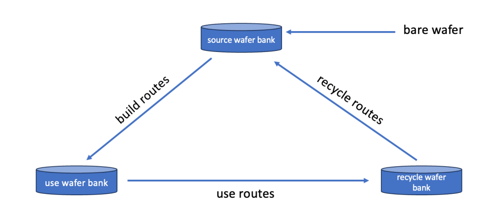
Lets walk through the cycle on an hypothetical example for the following case:
After a maintenance event on a dry etch tool there needs to run a particle test wafer as well as an etch rate test wafer to confirm the the chamber is in spec for release to production. In order to so they need to be ready for use when the maintenance work is done.
Lets assume:
1. the particle test wafer needs to be of a certain cleanliness before it is used on the etch chamber
2. the etch rate wafer needs to have a known thickness of a certain filmBuild routes
to prepare or “build” these wafers the following 2 routes might be used:
Particle wafer route:10 – start wafer from source wafer bank
20 – clean wafer at wet clean tool
30 – measure particles at metrology tool
40 – grade wafer – if below needed particle count -> o.k. to use
50 – store wafer in use wafer bank
Etch rate test wafer route:10 – start wafer from source wafer bank
20 – clean wafer at wet clean tool
30 – measure particles at metrology tool and if good:
40 – deposit needed film on wafer at deposition tool
50 – measure film thickness
60 – grade film thickness – if good:
70 – store wafer in use wafer bankSince it takes time to “build” these wafers it is clear that this has be done in advance of the actual use else their is high risk that the test wafers are not ready in time.
Another aspect of the build process is that of course not a single wafer will be build, but instead full lots (like 25 wafers per carrier).
This also means in the use bank there are likely multiple ready to use wafers sitting in the same carrier.Use routes
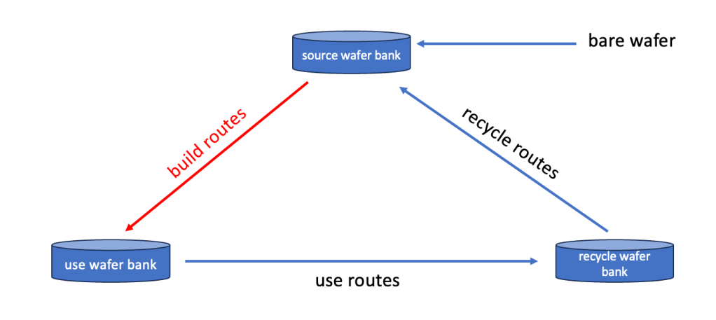
To be able to actually “use” the 2 wafers for our post maintenance check, again a couple of things need to happen, which is typically managed by using “use routes” examples for or 2 wafers could be:
Particle Test wafer
10 – start wafer from use wafer bank
20 – split out 1 wafer into an empty new carrier
30 – run (cycle) wafer through the etch chamber
40 – measure particles added by the etch tool
50 – if particle adders are in spec – set flag in MES to “good to use in production”
60 – grade wafer – if still good for next use – send back to use bank, else
70 – store in recycle wafer bankEtch rate test wafer
10 – start wafer from use wafer bank
20 – split out 1 wafer into an empty new carrier
30 – run etch rate recipe at the etch chamber
40 – measure new film thickness at thickness measurement tool
50 – if etch rate is in spec – set flag in MES to “good to use in production”
60 – grade wafer – if still good for next use – send back to use bank, else
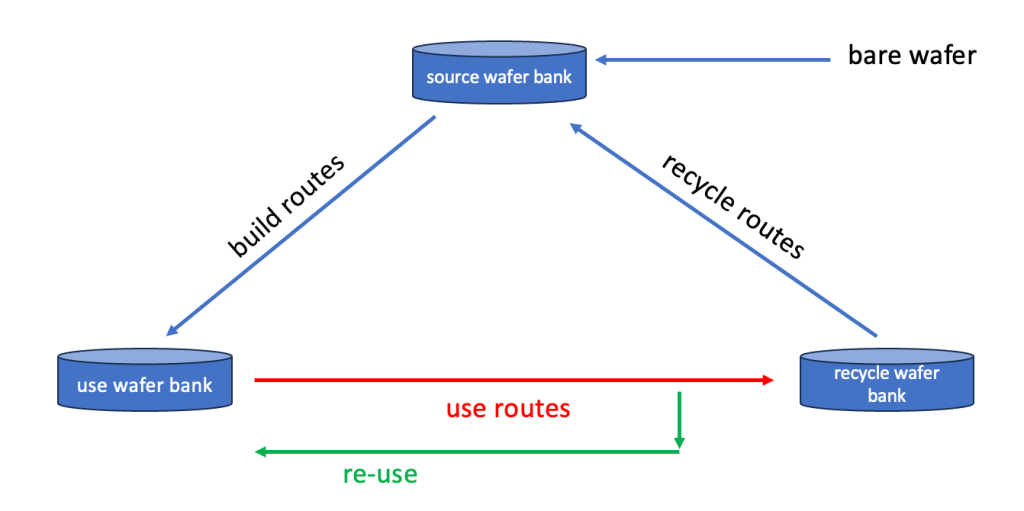
70 – store in recycle wafer bankbased on the option of directly re-using an already build and used wafer the model becomes this:
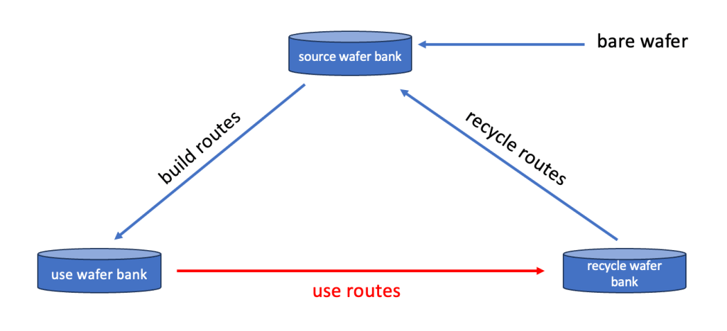
Recycle routes
Lastly, but also very important – what to do with all the used wafers ?
For cost saving reasons most FAB’s have implemented in-house recycling flows to “clean” the used wafers and put them back as “like new bare” wafers in the source wafer bank
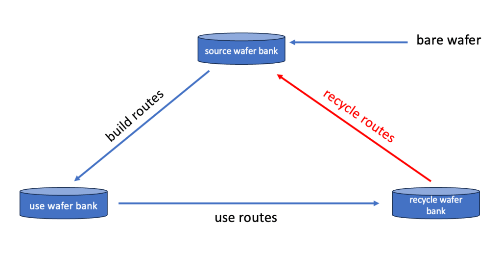
For our 2 wafers (very likely in one lot/carrier together with other similarly used wafers sitting in the recycle bank) these routes could look like this:
used particle test wafer:
10 – start lot from recycle wafer bank
20 – clean wafer at wet clean tool
30 – measure particles at metrology tool
40 – grade wafer – if below needed particle count -> o.k. to use as “like new”
50 – store wafer in source wafer bankused etch rate test wafer:
10 – start lot from recycle wafer bank
20 – completely etch all remaining film from wafers at etch tool
30 – measure film thickness ( should be zero now)
40 – measure particles and if good
50 – store wafer in source wafer bank
These examples of routes are of course extremely simplified. I conveniently ignored to describe all the needed lot ID and product ID changes which are involved in this life cycle, but it should be good enough to illustrate the principle.
A key part of the test wafer process is the frequent change of wafers into different carriers. Typically these happen at least at the read marked “points” in the flow:
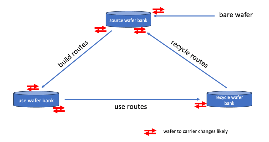
Depending on how automated a FAB is this can be a massive effort and drives a lot of operator time. Therefore the test wafer process it is a prime target for automation efforts.
Final thoughts
There are many more aspects of how to model and run test wafers in a FAB, which all have their pros and cons as well as depend on general policies the FAB applies: A few of the more interesting ones are:
- Do the FAB policies and CIM system capabilities allow multiple different lots to be stored and transported in the same carrier ?
- How is test wafer ownership organized ? For example: do different areas manage their own test wafers or is it allowed to share for example particle test wafers with other areas ?
Depending on how this is organized it might reduce the overall amount of test wafers – or not. - How are minimum and maximum stock levels at the 3 wafer banks defined ?
- How and where are test wafer lots stored and tracked from a physical location point of view ?
“somewhere in one of the 3 shelves over there” vs. in a stocker – makes a big difference - Do FAB policies require fresh pre-measurement data before each use or can old post measure data be used to save time. And if yes, how old can the data be ?
- How often can wafers be recycled before they are not usable anymore ?
- What is the scheduling/dispatching logic for test wafers on build and recycle routes at process tools which also run production lots ?
- Is there regular test wafer WIP level and test wafer aging reporting set up ?
- Who owns the test wafer “business” in general ? Operations ? Engineering ?
- Are there dedicated engineers assigned to manage test wafers in the FAB ?
- What happens if a test wafer in use case comes back with data out of spec ?
Is it a simply re-do of the test wafer run – and if yes – is it automatically a second run ? - How many of the traditionally on test wafers done tasks can be done directly on product wafers (at what risk) to save test wafers altogether ?
- Is there data available on how often process equipment has extended down time due to no test wafers ready ?
- Which of the test wafer uses cases are “gating” – meaning the process tool tested has to wait until post measurement data is available ?
- What is the frequency of scheduled test wafer runs? daily, weekly, every 10 days …
- How advanced is the deployment of run to run controllers to avoid seasoning, warm up or send ahead wafers ?
I’m sure I missing a lot more aspects. One thing is clear, test wafers have a huge impact in a FAB – and based on everything written above this is not a small “Friday afternoon” task.
To manage this “zoo” successfully:
1. test wafers need to have the same importance as any other wafer in the FAB
2. a well defined set up in MES is needed
2. ownership needs to be defined
3. engineers need to be allocated / dedicated
4. automating the kitting, de-kitting as well as the transport of test wafer carriers will significantly improve efficiency (spoiler alert: Fabmatics’ TESTWAFERCENTER can help with exactly that)Happy Test Wafering 😉

-
Test Wafer, part 2
First of all, thanks to everybody who participated in the test wafer usage poll in the last post. I received some decent feedback and below are the results:
For 150 and 200mm FABs (based on 15 data entries)

The data show that test wafers play a massive role in the day to day FAB business. Most FABs have significant amount of test wafers as well as allocated carriers to test wafers.
For the 300mm FABs:

The general theme is the same, but there are 2 important remarks to make:- there were only 5 feedback votes – it seems in 300mm the overall competition might be tighter and the willingness to share data is limited – so the data above might be not a good reprensentation of the 300mm situation overall
- there were 2 data sets indicating less than 10% of carriers are used for test wafers – this is interesting since the overall test wafer percentage in the FABs is still high.
My guess is that in 300mm FABs with the high material transport automation capabilities there might be single wafer stockers in use to store test wafers outside of FOUPs.
Overall, the data set from the polls show a picture which I was expecting. Test Wafers are plenty in the FABs and they consume a lot of carriers as well as storage space. Here is a high level thought to get a feeling for real numbers:
Let’s assume a small/mid size wafer FAB has the following WIP related indictors:
- 10,000 wafer starts per week
- average 30 mask layers
- 1.8 days per layer cycle time on product lots
- average lot size 24 wafers for product lots
That will translate into an overall FAB production WIP of about 80,000 wafers, which will sit in about 3,400 carriers. Based on the poll data that would also mean that this FAB has an additional 50,000 … 90,000 test wafers sitting in 2,000 … 4,000 test wafer carriers.
I think this is mind boggling – at least compared to how much is typically talked and written about test wafers and test wafer management.
So how come that there are such massive amounts of test wafers in the FABs ? For sure it has to do with the impact of test wafers – especially when they are missing. ( see the part 1 of the test wafer post)
In my next post – which will be the 3rd and final part for the test wafer topic – I will discuss some of the common strategies and methods:
How to have control over these massive amounts of test wafers and test wafer carriers and how to make sure that equipment uptime is not (too often) impacted by missing test wafers.
-
Test Wafer , part 1
Inspired by the recent LinkedIn post from Fabmatics about the TestWaferCenter (LINK)
I thought it is time to look a bit closer at the general topic of “test wafers”. So what are test wafers ?
To keep it simple I will use the term “test wafer” for any non-product wafer in a FAB. Test wafers are the unsung hero in every FAB – almost like electricity and water in your home – you really only notice them when they are not available. Typical variants of non-product or “test wafers” are:
- wafers to qualify / re-qualify a process equipment after a maintenance event like thickness, etch rate or particle measurement wafers
- conditioning wafers, used to ensure process conditions in an equipment are ready to run product wafers, for example after longer idle times or recipe changes
- filler wafers typically used in batch furnace equipment to fill up empty wafer slots in the process boats
- monitor wafers – which are processed in parallel to product wafers in an process equipment to measure certain process results
- mechanical handling wafers used to teach / re-teach robots and general wafer handling inside of process equipment
- calibration “golden” wafers used to re-calibrate metrology equipment
In contrast to these wafers there are of course the product wafers, which are the wafers most people care about in a FAB:
- regular product wafers ( will contain at the end of the process real chips)
- R&D wafers – future product wafers ( will contain at the end of the process real chips)
- short loop wafers – to experiment and learn at certain segments of a real product process flow
The interesting thing about test wafers: these have massive impact on the overall FAB productivity:
a) in a positive way – by being always available when needed
b) in a negative way – by being not available when needed – for example after maintenance of a process equipment – missing qualification wafers will extend the equipment down time and therefore reduce the FABs capacityIn one of my past roles at a wafer FAB – every once in a while in the morning meeting we had reports about process equipment being extended down, since the needed test wafers were not available (in time) – obviously not a good situation to be in.
The fix to this situation seems easy – have the test wafers ready … ?!
But what does this mean exactly and how to make sure that this indeed works as desired ?
Unfortunately, the topic is very complex and it starts with the typically very large amount of different types of needed test wafers. The challenge is not only to have “a test wafer” available when needed, but the “right” one. To ensure the availability of all needed types of test wafers, FABs will have stock levels of these wafers and if summed up it can add up to impressive overall numbers of test wafers in a FAB.
One useful indicator on how complex the test wafer topic in a FAB is, is the ratio between product wafers and test wafers.
For example:
if a FAB has a total product WIP of – let’s say – 100,000 wafers and in parallel has also about 20,000 test wafers “sitting” in the FAB the ratio would be 100,000 : 20,000 or 1 : 0.2if a FAB has a total product WIP of 100,000 wafers and in parallel has also about 100,000 test wafers “sitting” in the FAB the ration would be 100,000 : 100,000 or 1 : 1
In my 29 years in semiconductor I have seen vastly different product to test wafer ratios and I’m super curious what the situation looks like nowadays. The need for test wafers also is a function of the criticality of the process nodes running in a FAB. For that reason I divided the poll below into 2 groups:
- 300mm FAB – assuming that these mostly run more advanced process nodes
- 150 and 200mm FAB – typically running more mature and legacy process nodes
If you are working in a 300mm FAB:
Similarly, if you are working in a 150mm or 200mm FAB:
I will share the results of these pools in my next blog post – very much looking forward to see the numbers !
Test wafer management does come with one other challenge: low number of wafers in a carrier.
No matter which carrier type your FAB uses:
- 300mm FOUP
- 200mm SMIF pod with a cassette inside
- 150mm or 200mm box with a cassette inside
- 150mm or 200mm open cassette
Typically product wafer carriers contain more or less close to 25 wafers per carrier, while test wafer carrier very often do only have 1, 2 or 3 wafers inside.
It means that often a surprising large amount of carriers is occupied by test wafers and that requires a very controlled carrier management to not run out of available empty carriers (and storage places). I’m curious here as well, what is the overall situation nowadays in the FABs ?
If your are working in a 300mm FAB:
Similarly, for a 150mm or 200mm FAB:
Please provide some feedback using the polls if you have the needed data available. It will help to focus in my next blog post on the right topics.
If your not subscribed to my blog yet :
-
ASMC 2024
The Advanced Semiconductor Manufacturing Conference – short ASMC – will take place at a new venue this year. After many years in Saratoga Springs, NY this years conference will take place in Albany, NY.
Conference registration is open now and the reduced early bid fee is available only until 04/01/2024 !
direct link to the Conference webpage: LINK

I’m looking very much forward to this event for 2 reasons:
- Spring in Upstate NY is a beautiful season to meet and gather with industry peers from all over the world – if you come a few days early you have a chance to visit the Albany Tulip Festival

- listening to the latest news and trends in the semiconductor manufacturing world
The Conference Committee has put together a great line up of keynotes, technical sessions, panels and a poster reception. Here are a few of my personal highlights:
- Keynote from Vijay Narayanan (IBM fellow) about innovation in semiconductor in the AI area
- Keynote from Missy Stigal (VP Operations at Wolfspeed) about SiC
- Keynote from Robert Maire (President Semiconductor Advisors) – always a “must see & hear” about the latest developments in the industry
- Panel Discussion—Talent Pipeline: Building a Sustainable and Diverse Semiconductor Workforce
- Session 8: Smart Manufacturing + Industrial Engineering 1 – LINK
- Session 16: Smart Manufacturing + Industrial Engineering 2 – LINK
- Session 18: Factory Automation – LINK
Looking through old notes I realized ASMC 2024 will be my 20th ASMC – unbelievable how fast time flies!
ASMC 2004 took place in Boston, MA and I was a young and nervous engineer presenting my 1st paper – what a journey over the last 20 years !If you are curious what my paper was about in 2004:
But now lets look forward to ASMC 2024 – I hope I have the chance to meet many of you in person in Albany, NY in May !
-
THANK YOU 2023
Amazing how fast another year went by. I want to use the opportunity to say THANK YOU to all the followers and readers of my block. 2023 was again a very dynamic and successful year. Lots of good interaction on the subject of Factory Physics and Automation.
I wish you a great Holiday Season and hopefully I will see you all back in 2024 – here on these pages.
Speaking of 2024 – it already makes the news:
the 2024 Edition of the Innovation Forum in Dresden, Germany has lined up a great agenda: LINK
and the registration for this event is open: LINKalso – Gartner, Inc. forecasts that 2024 the semiconductor industry will be back on the growth track:
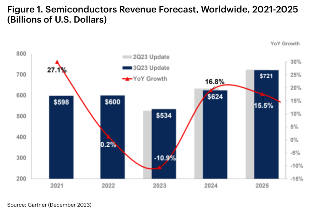
full article is here: LINK
-
Maintenance and FAB productivity
Today I save a lot of time typing – since there is a great article on the topic – written by McKinsey and Company.
As I have written about this topic in earlier posts – I can only recommend to read this piece as well:
On a related topic, a good old friend and former colleague of mine – Subramanian “Subbu” Pazhani – provided me as a guest author to the blog a great paper with the title
Analyzing Fab Bottlenecks – a Quantitative View
If you are interested to dive in a bit deeper on the impact of variability on equipment – hence FAB – performance, please have a look below.
Subbu is teaching Factory Physics at the NC State University in Raleigh, NC and a long time Factory Physics practitioner in the semiconductor industry. -
Impact of “time links” or controlled queue times
Today I like to discuss another potential FAB performance detractor – time links or controlled queue time zones. These got introduced to the more advanced process flows to avoid negative impact from long queue times between different process steps. Typical reasons for controlling length of queue times between steps are possible unwanted oxidation or corrosion on the surface of the wafer. These can have negative impact on overall wafer / chip yield and/or reliability.
In the ideal case the process engineering team has detected such time sensitive behavior between process steps and created charts like the one below:
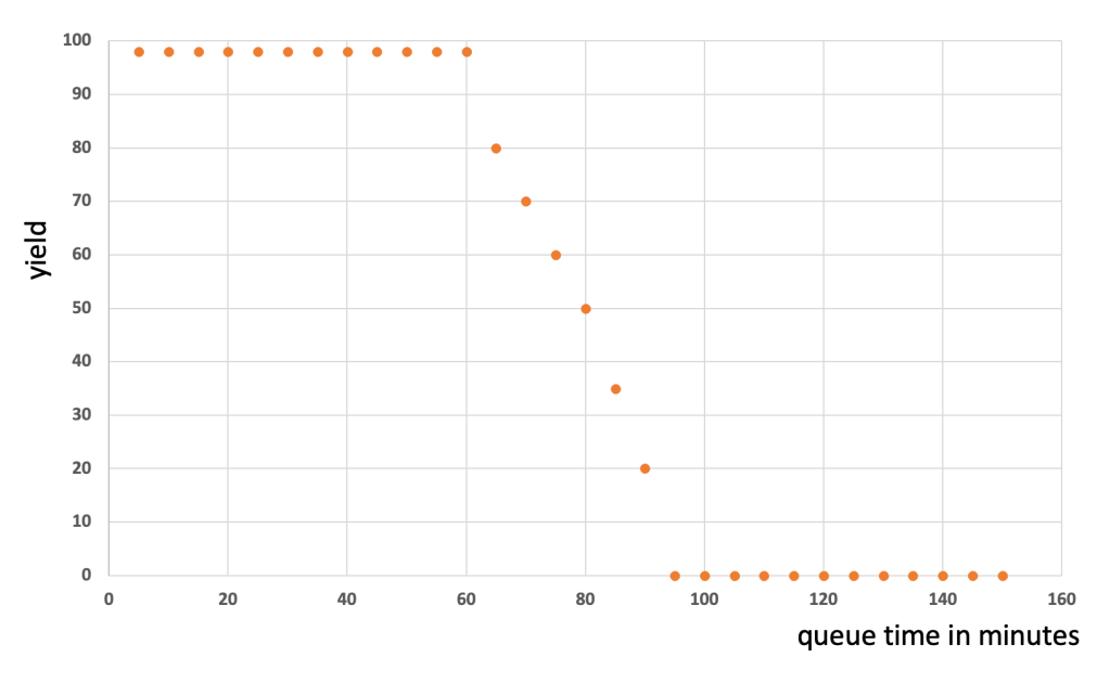
Based on the shown graph there is clearly a cliff starting after 60 minutes of queue time. The process team will very likely request from the manufacturing team that lots never wait longer than 60 minutes at in this zone. To be on the safe side the request might even be max. 45 minutes.
Lets have a look how such a time link zone is typically defined:
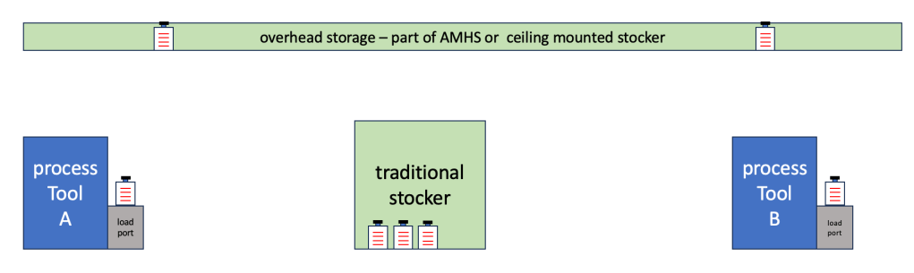
Time link zones are typically defined by a zone between a “trigger step” and the “target step”. The trigger step is the step in the process flow where the time link zone starts. A typical definition can be:
– the queue time starts, when the lot receives a operation complete – meaning all wafers at the trigger step on process tool A are completed and back in the carrier. The time would end when the lot receives an operation start at the target step on the target tool – in the picture above the process tool B.The idea is that all the time the lot / carrier is spending in transport, waiting in storage locations is counted towards that maximum allowed queue time, which should not be exceeded.
How can manufacturing manage this ?
In a nutshell: a lot will be only started at the trigger step / tool, when there is a guarantee, that the lot can be started at the target step within the given time boundary (in my example 45 minutes). This sounds pretty simple, but involves a lot of calculations and scheduling.
- on how many tools can the target step be processed
- how much WIP is in front of the target tool group waiting
- how long is the transport time between trigger and target step
- are there other higher priority lots in the time zone
- … many many more
There are many different ways in the FAB to manage this – from simple KANBAN approached to neuronal network based solutions. All of them have on thing in common: protect the wafers from too long wait time between trigger and target step. In a nut shell: the WIP flow will be controlled, which typically means slowed down.
There are 2 points in a flow where this happens:
1. for all time link lots at the trigger step – it will only be released onto the trigger steps if the zone is “empty enough” – hence each time the zone is not ready – the lot will wait.2. other lots waiting on the target tool, which are not in a time link zone ( on a different step in the flow) will have to give a time link lot priority – and therefore they have to wait even longer.
How big the overall impact on the FAB performance will be depends on a lot of things. Prominently these:
- shortness or length of the time link zone
- total number of different time link zones in a flow
- how risky the scheduler manages the time link zone
1. length of a time link zone
To define the “best length” is a tricky task. From a yield point of view shorter is better. From a manufacturing point of view longer is better. But not only that. In reality the yield degradation curves do not look that well defined like in the example from the top. Where to put the limit for the one below ?
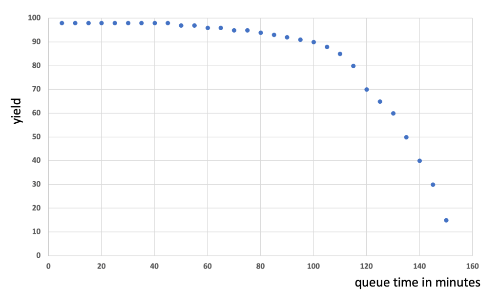
Set the max allowed time to 45 minutes to be super safe – but likely have massive WIP flow impact ?
Set it for example to 80 minutes and take a yield hit ?
Another interesting aspect is the definition of the start and end time of the time link zone itself. The above used method of operation start of the target step and the operation complete of the trigger step is often not good enough for very sensitive processes.
Technically, the “bad environment influence” on the lot starts when the 1st wafer of the lot is finished with processing at the target step and is back in the carrier waiting for the other wafers of the lot.
For this 1st wafer the queue time ends, when it is back in the process chamber of the target step. The definition of the time link zone would be then: process complete of the trigger step until process start of the target step – at wafer level – not the lot level !
To manage time links on wafer level is a much harder challenge.
2. total number of different time link zones in a flow
Managing a single time link zone can be challenging, but if there are multiple zones with multiple steps and tool groups involved – it can become a challenging mathematical problem very fast.
Rule of thumb: More zones, more challenges and more impact on FAB productivity
Most mature processes often have only 1 or 2 time link zones – usually in the gate oxide and/or gate poly steps. Advanced process flows can have hundred or more time link zones!
3. how risky the scheduler manages the time link zone
In complex time link zones is no 100% guarantee that all lots “make it safely” in time to the trigger step. Too many factors and their variability will prevent the perfect solution.
A simple example is: If a target tool goes down, while there is planned WIP for this tool in the time link zone.
Therefore most algorithms use settings to calculate the probability of a lot making it in time to the target step. And the settings for these depend on many factors, again.
Rule of thumb: the higher the probability is set (lower risk) the more impact on FAB performance
Summary
Any time link zone in a flow will have impact on the FAB performance – just by the fact that every once in a while a lot has to wait at a target step.
How much the impact is depends on how much the FAB is willing to “pay for” avoidance of impact. Payment comes in one or more of these “currencies”:
- plan with lower tool utilization to provide buffer capacity
- invest in advanced scheduling (software, server, people)
- invest in Nitrogen purged storage solutions to extend the possible queue time
for example: OHT or stocker purge upgrades LINK
A great additional source on the subject of managing controlled queue times is the
FabTime Newsletter: Vol. 24, No. 2: Managing Time Constraints between Process Steps in Wafer Fabs
LINK -
MES & Industry 4.0 Summit in Porto, Portugal
What an event it was ! Critical Manufacturing organized on outstanding event – and I hope there will be a second one not too far in the future. About 500 experts met in Porto to discuss digitization and Industry 4.0 efforts. To me it was mind-blowing how much is going on in this area.
A key observation I had over the whole 2 days: There are big differences in how much progress different industries and companies have made so far.
One of the bigger challenges discussed multiple times is: How to calculate a realistic ROI for all the upfront cost to achieve a full digitization of a company or is this just a basic business enabler for future success ?
A first step to this journey is to understand where does your company stand today ?
I found this particular table from Jan Snoeij’s presentation very interesting to assess what manufacturing maturity level a company may have reached (1. being the lowest, 5. being the highest).

It is impossible to blog about all the great presentations and talks during the 2 days, but here are some of my favorites:
Jeff Winter Keynote: Transforming Manufacturing with Industry 4.0 – runtime about 38 minutes
Nicholas Leeder, The Smart Industry Readiness Index – runtime about about 30 minutes
Didier Chavet: The Role of AI in Manufacturing: Use Cases from the SEMI industry – runtime about 25 minutes
Francisco Almada Lobo: Stairway to Industry 4.0: a journey through hype and reality – runtime about 33 minutes
I had the honor to moderate a panel discussion on the topic of “Role of MES and IIoT in building resilient and data-driven enterprise” – runtime about 60 minutes
All presentations and recordings from the summit are available here: LINK
-
ASMC 2024 – call for papers
Next years Advanced Semiconductor Manufacturing Conference (ASMC) will take place in a new location. After many years in Saratoga Springs, NY ASMC 2024 will take place in Albany, NY.
Every year over 400 experts from the semiconductor industry meet at the conference to discuss and exchange about manufacturing challenges. Due date for this years call for abstract is October 10.
direct link to ASMC 2024 website: LINK
call for abstract flyer with all the key facts:
Since many years the conference is organized by a group of industry experts and seasoned semiconductor manufacturing professionals (LINK), all abstracts and papers are peer reviewed. Most of the committee members will be in person in Albany, NY – another great reason to attend to exchange with experienced peers in your field.

-
MES Summit in Porto, Portugal
I’m usually writing here about Factory Physics and (soon) Factory Automation topics. One major aspect of both is to have good data to understand the behavior of your FAB. Modern FABs are extremely complex “eco systems” and operating at “best performance” possible needs fast access to the “right” data. Key for this is for sure an advanced MES and more and more companies adding IoT elements to it.
I’m honored to moderate an expert panel at the MES Summit in Porto, Portugal which will dive into the IoT aspect

I will post about the event once I’m back.
It is still not to late to register : LINK
Here is a direct link to the agenda: AGENDA
Maybe I meet you in Person in Porto ?
-
2024 Innovation Forum for Automation
Today just a quick heads up: next years Innovation Forum for Automation will take place in Dresden, Germany on January 25 -25.
This year, there is a call for papers, so if you have an interesting project, problem or problem solution in the area of factory automation – the Innovation Forum could be a great stage for it:
Potential topics:
- Automated material handling & robotics
- AI, new automation approaches
- Energy efficiency /sustainability
- Shop floor automation for legacy Fabs
- Dispatching & scheduling
- Predictive manufacturing
Relevant Industries:
- Semiconductor
- Electronics
- Automotive
- Renewable Energies
please have a look here for the call for papers: LINK
and here is some background info on the Innovation Forum in general: LINK
-
Data is the new oil – or is it skilled workforce ?
I just came back from the 2023 ASMC in Saratoga Springs, which was packed with 15 technical sessions and lots of great presentations. One topic was in the air throughout all the sessions – will the semiconductor industry have enough skilled operators, technicians and engineers ? Almost all keynotes brought this point up and there more I look at it the more I think the industries biggest problem in the next 5-10 years is the lack of skilled people.
Below are a few take outs from the presentations:
keynote Dr. Thomas Morgenstern, Infineon
keynote Thomas Sonderman, SkyWater Technology

panel discussion, Rick Glasmann, The MAX Group
keynote Robert Maire, Semiconductor Advisors
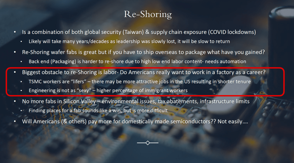

Robert Pearson, RIT

As a matter of fact, Roberts’ presentation sums up the situation perfectly and I got his permission to post it here:
Even the panel participants displayed a mirror image of the workforce situation. 3 out of the 4 panelists were seasoned Equipment Engineering / FAB veterans in contrast to the young AI / data expert. It really seems that the mechanical / electrical hands on work is slowly going extinct.
As one panelist shared with the audience: ” … I do have 3 kids, none of them want to work in the semiconductor industry …” asking about the why: ” … dad, look at you, you are always late back home, your are always stressed, the phone never stops ringing – why do I want to choose a life like this ? …”
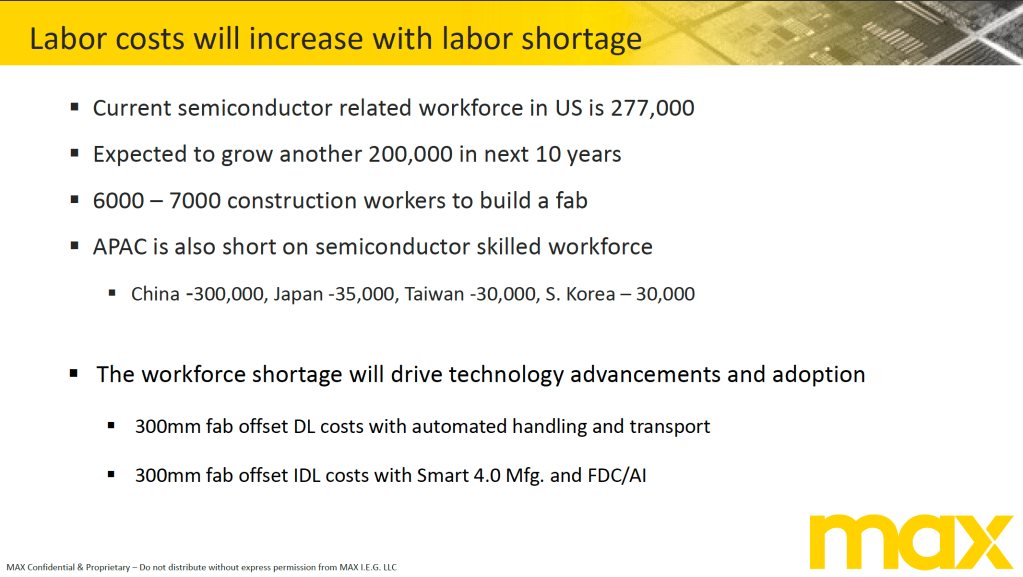
The topic is serious – I think existentially serious. The semiconductor industry is extremely capital intensive and will only survive if the equipment in the FAB is running 24/7. Based on the numbers – showing the needed additional skilled workforce – it seems there will be many, if not all factories facing output and efficiency losses. But how much ?
Most forecasts show a delta of about 200,000 workers over a base of about 300,000 existing workers – that is a 40% gap. Depending on the specific field where the workforce is missing the impact will be different:
- missing operators in manual FABs will have massive direct impact – tools will not be loaded / unloaded in time and therefore there is direct loss in capacity and cycle time
- missing process technicians will have impact on hold lot release and overall process stability and therefore impact yield and reliability
- missing maintenance technicians and engineers will directly lead to less equipment uptime and lower equipment stability, both directly impacting FAB output, yield and reliability
- missing process engineers will lead to reduced process improvement work as well as to less stable manufacturing processes
- the list goes on and on
What will be the economical impact of all this ?
The total US semiconductor industry revenue in 2022 was in the neighborhood of $275 billion. If I just assume that a 40% shortage in skilled workforce will have a 10% overall impact (which I think is a extremely conservative estimate) that would mean, in the next 5 years there will be a loss of 5x $27.5 or
$137.5 billion
Even if my back of the napkin calculation is wrong by a factor of 2 or 3, this number is mind boggling – and it appears “nobody” really seems to take serious action – Why is that ?????
I guess, factors are ” it will affect not my company, since so far it has been not a major problem …” or ” .. if worst comes to worst, we can always raise salaries and get people from across the street …”
Nevertheless, if some companies might be less impacted, that means others are even more in a shortage. For the overall industry both scenarios are not good. The magic question is how to make jobs in semiconductor attractive again ?
Remember:
” … dad, look at you, you are always late back home, your are always stressed, the phone never stops ringing – why do I want to choose a life like this ? …”
Being myself a long time semiconductor addictive I fully can relate to that. It might be easy to say ” the young folks nowadays don’t like to work hard anymore …” – but false or true that will not change things. The semiconductor industry will be only more attractive for new technicians and engineers, if we change within the industry, what is seen as the problem by the next generations. The companies, which react and change first will have the best chances to again attract people.
Let me throw out a few possibly controversial thoughts here:
you are always late back home
Long hours have been a sign for hard work for way too long. If people need to stay on regular basis long hours, thats a sign for understaffing or bad organized / trained organizations. Unfortunately, reducing headcount numbers is seen as the easiest way to reduce cost. Too often, the quarterly hunt for good numbers – to keep Wall Street happy – leads to cuts, which are counterproductive in the mid and long run. Frequent downsizings – which are not uncommon in the semiconductor industry – are not a strong signal to attract the next generation of technicians and engineers.
–> rethink overall human resource strategies and become much more people centric (vs. pure head count efficiency, short term thinking)
–> incorporate impact of missing or not well trained workforce in all business model calculations to put hard $ numbers behind the effects (vs. assuming, people will be there when needed and set availability to 100%)
your are always stressed
Stress typically is generated, when people feel under pressure, since they can not control their job, but are controlled by overwhelming tasks and timelines. Outside of the general not enough people issue, key reasons are not enough know-how, training and resources to successfully do the job.
–> massively invest in training and standardization, people need to know what and how to do it
the phone never stops ringing
This is another “evil’ of the modern time: Always on, always connected and no clear rules for protecting employees personal time. This might be part of the general understaffing problem, but also not having enough experienced people, who can share the burden of on call and critical problem escalation support. During COVID people realized that there is also a life outside of work. Enjoying time with family becomes more and more important. If employers do not react people will leave or not even join to begin with.
–> how about guaranteed personal time with no contact from work and possibly a general 4 day work week ?
(imagine the company across the street starts to offer 4 day work week to attract people)
I still think the semiconductor industry can be very exiting to work in: There is plenty of fancy high tech “stuff” to be proud of, to be involved for all levels of education. Salary needs to be at least somewhat competitive. If people get rock solid training and career path, there should be no reason why people do not choose a career in semiconductor. Employment will be almost guaranteed in the next 10-15 years, looking at all the shortages.
I think these are the main levers to make semiconductor industry attractive again:
- massive image campaigns to the greater public and schools
- create opportunities for young people to understand what it means to work in a FAB
- community colleges and universities to offer the needed classes to study what is needed
– input and funding to come from the semi industry - seriously care about your people and get rid of the 24/7 grind with rules and appropriate staffing
- define semiconductor industry wide accepted job standards, which describe skills sets needed and certification levels
- training, training, training and clear career path visibility
This all will only happen if driven by the ones who have the problem in the first place – the semiconductor industry and universities that teach semiconductor engineering itself. It is not that the FABs should or can pay for everything themselves, but they need to start driving activities yesterday. Last but not least, programs like the CHIPs Act clearly need to involve workforce development with significant amounts, since else all the new FABs will not run as productive as planned . The result will be, that the attempt to bring semiconductor manufacturing back into the US will fail.
Super curious what you think about all this – please comment !
2 responses to “Data is the new oil – or is it skilled workforce ?”
-
Wie wahr, wie wahr.
Es bleibt spannend. Und die Frage nach dem Personal und anderen Resourcen bleibt offen.
Würde mich freuen, wenn wir uns bald mal wieder sehen würden.
Mit freundlichen Grüßen/best regards
Thomas Leitermann
+49 172 79 37 194
>
LikeLike
-
Very true. Many companies have not yet realized that it will become ever harder to get skilled employees.
Good point that new hires are not 100% up to speed immediately. For a maintenance technician the learning curve is 2 years. We need to factor this into financial considerations about “head count”. It is not only heads, it is skill. Lack of skill might become “apparent” only indirectly through yield excursions or too long maintenance times.LikeLike
Leave a comment
-
ASMC 2023
The Advanced Semiconductor Manufacturing Conference in Saratoga Springs is just one month away !

I’m looking forward to meet many industry experts and discuss Factory Physics topics in person. Here are some of my personal Agenda highlights:
- Keynote: Salvatore Coffa from STMicroelectronics – Silicon Carbide
- Keynote: Thomas Sonderman from SkyWater Technologies – US Chips Act
- Panel Discussion: Unintended Consequences of Government Subsidies on Moore’s Law and the Future of Semiconductors
and of course plenty of interesting technical presentations – these are some of my favorites:
- How to Teach Semiconductor Manufacturing and Why it is so Difficult
- Impact of Effective Technical Training in a Semiconductor Manufacturing Facility
- Automation in R&D: complying with contradictory constraints of seemingly incompatible world
- Granularity of Processing Times Modeling in Semiconductor Manufacturing
- Deploying an Integrated Framework of Fab-wide and Toolset Schedulers To Improve Performance in a Real Large-scale Fab
Hope to see you in person in beautiful Saratoga Springs, NY !

- Keynote: Salvatore Coffa from STMicroelectronics – Silicon Carbide
-
Product Mix and FAB performance
Semiconductor manufacturing is a highly complex and dynamic industry that requires constant innovation and adaptation to meet the changing needs of customers. One of the biggest challenges in this industry is managing changes to the product mix, which can have a significant impact on the overall efficiency and effectiveness of the manufacturing process.
Product mix changes can occur for a variety of reasons, such as changes in market demand, new product introductions, and shifts in technology. These changes can have a ripple effect throughout the entire manufacturing process, impacting everything from sourcing and procurement, to production and logistics.
One of the major challenges of product mix changes is the need to quickly and efficiently re-configure the manufacturing process to accommodate the new products. This requires significant coordination and collaboration across multiple departments, including engineering, procurement, and production. Additionally, changes to the product mix may also require the use of new or different equipment, which can add further complexity to the process.
Another challenge is managing inventory and supply chain logistics. With changes in product mix, the demand for certain raw materials and components may fluctuate, requiring adjustments to inventory levels and procurement strategies. Additionally, changes in product mix can also impact shipping and delivery schedules, requiring careful coordination with customers and suppliers.
Overall, managing product mix changes in semiconductor manufacturing is a complex and dynamic process that requires a high degree of coordination and collaboration across multiple departments. It is important for companies in this industry to have a robust and flexible manufacturing process that can quickly adapt to changing product mix requirements, in order to remain competitive and meet the changing needs of customers.
O.k. – the text block above was generated by OpenAI’s ChatGPT.

I asked it (?) to “… write a short article about the complexity of product mix changes in semiconductor manufacturing …”
pretty impressive, especially because it took only about 10 seconds – the next text block was it’s second try:
Semiconductor manufacturing is a complex and constantly evolving industry, with a wide range of products that are produced using a variety of different processes and techniques. One of the most significant challenges faced by manufacturers in this industry is the complexity of product mix changes.
When a manufacturer wants to change the product mix of its semiconductors, it must consider a variety of factors, including the specific processes and techniques required to produce the new products, the availability of equipment and materials, and the costs and risks associated with the change.
One major challenge in changing the product mix is the need to retool and reconfigure manufacturing equipment. This can be a costly and time-consuming process, as manufacturers must purchase new equipment and train employees on how to use it. Additionally, the process of retooling can also lead to downtime and disruptions in production, which can have a significant impact on the bottom line.
Another major challenge is the need to secure and maintain a steady supply of materials, as well as the need to dispose of any remaining materials that are no longer needed. This can be a difficult and costly process, as manufacturers must navigate a complex supply chain and ensure that they have the necessary materials on hand to produce the new products.
Finally, manufacturers must also consider the costs and risks associated with changing the product mix. This can include the costs of retooling and reconfiguring equipment, as well as the potential loss of revenue if the new products do not sell as well as expected. Additionally, manufacturers must also be prepared to address any potential issues that may arise during the transition, such as quality control problems or supply chain disruptions.
Overall, changing the product mix in semiconductor manufacturing is a complex and challenging process that requires careful planning and execution. Manufacturers must weigh the costs and risks associated with the change against the potential benefits, and be prepared to address any issues that may arise during the transition.
I promise, the following contains only 100% of my own thoughts …
One of the more tricky aspects of optimizing factory performance is understanding the true impact caused by product mix changes. The key problem here is the level of complexity to:
- understand
- calculate and/or estimate
- drive actions to reduce the impact
Unfortunately there is no “one size fits all” rule to deal with this – other than:
The higher the product mix is in a FAB – the more likely there will be performance loss.
Almost 20 years ago I was confronted the 1st time with the problem of increasing product mix. I visited a factory which had recently gone from an almost mono culture FAB to a factory running now 10+ different products. FAB cycle times increased, output went down -all this at the same wafer starts level like the years before – and the management wanted to understand what is going on … (it seems that ChatGPT today has more “understanding” about this than the management 20 years ago)
Experienced factory physics practitioners will likely smile about this, but without a good understanding of the effects of changing product mix plan and actual results will very likely not be in sync.
Let’s try to dig into the topic a bit. First we need to define what do I mean with a product. In the real world there are various levels of differences between a product and another one. Unfortunately different companies have different naming conventions for that. I will use this definition: A product is different to another one, if at least one processing or metrology / test step is different.
For example: if the manufacturing of a wafer leads to the exact same chips at the end of the wafer FAB processing and just get a different frequency capability assigned after testing ( like CPU’s) I would not call them different products. As soon as there are steps with different recipes in the flow – these are 2 different products.
The size of the impact scales with the number of differences: If 2 products with 500 processing steps have a different recipe on 12 steps are much more similar to each other, than a product which has 100 out of the 500 steps different.
What are they key effects of the differences :
- higher product mix will likely lead to smaller cascades on a process equipment since a recipe change might need additional setup times
- different recipes at the same equipment will likely have a different number of qualified tools (in the planned world but especially on the FAB floor)
- capacity planning no longer will work with simple static modeling approaches to reflect the real effective equipment and/or chamber dedication/availability
- batch building at batch tools will either lead to smaller batch sizes or to longer batch formation times
- higher number of products will likely increase the number of Litho reticles and therefore also increase reticle logistics and risk of “reticle not available when needed” scenarios
- back up reticle sets are likely less available for products with smaller WIP in the line
- small volume products tend to have higher metrology sampling rates (more often measured) since there is not enough “volume” statistics available
- achieving very high on-time delivery percentage is harder for very small volume products (if 1 lot gets scrapped, is this 33% of the total WIP ?)
- products with significantly different number of process steps (or mask layers) will likely create dynamic bottlenecks throughout the line due to different WIP arrival times
- higher number of different recipes on a tool might cause higher re-qualification time needs, which can impact tool availability negatively
- frequent changes in the product mix wafer starts will likely amplify the negative impacts of points 1. – 10.
How to deal with all of these complexities – especially if your FAB is going down the path of increasing product complexity ?
There are basically only 2 practical approaches to that:A) – reduce general FAB loading and see what happens (with no guarantee what will be the outcome)
B) – invest in IE systems and experts to be able to quantify, calculate and plan for the expected effectsI have seen both in the real world, with B having significantly better chances to hit cycle time, output and on-time delivery goals.
-
Rework and FAB cycle time
In todays post I will discuss the impact of rework on the overall FAB cycle time.
Rework can happen for various reasons and at different process steps. Most common it occurs after a lot has been processed at a photo step. The picture below shows a typical scenario
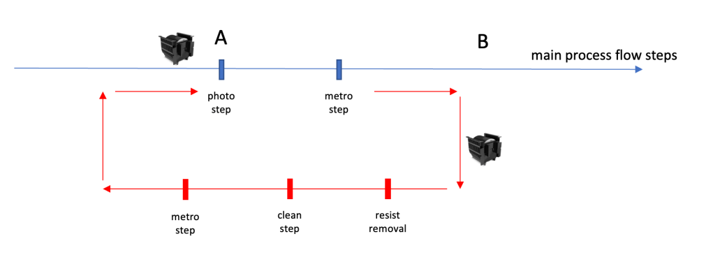
After a lot was processed at the photo step “A”, typically it will be measured at a metro(logy) step to see if the photo step was done within the desired specifications. If not, the whole lot or some wafers of the lot will be send into the red depicted “rework loop”.
There are different implementations of this in the real world. In some FABs the rework wafers will be physically split into a new carrier and the good wafers will wait at point “B” until the rework wafers are back. If this happens there will be additional sorter steps to execute the split and later the merge. These are not in the picture above, but both will consume wait time and process time, additionally to the times the rework wafers will need until they get back to point “B”
Another scenario in more advanced FABs will keep all the wafers in the same carrier and send the full lot through the rework loop. In this approach there are 2 possible execution flows:
- one where only the “bad” wafers get processed in the rework loop steps
- one where no matter what, the complete lot (all wafers) get the rework process.
Obviously all this different versions will have different cycle times – and therefore a different impact on the overall FAB cycle time.
In general any rework is a hint on missing stability in the overall process. Any rework move will consume capacity on the involved processing equipment. Typically this is most impactful on the Photo equipment itself. For example, if the average rework rate in a FAB on all Photo steps is 3%, this adds 3% of tool utilization and likely a few more cascade breaks to the dispatch list or schedule. Since Litho Tools are usually some of the highest utilized tools in the factory, this will drive their utilization even more up and therefore the average lot cycle time of all lots at the photo steps will go up. This effect was already discussed in earlier posts.
On top of this “higher Utilization drives higher cycle time” effect on the photo tools themselves, the effect might be there also on all other involved tools. The impact there is likely less, since the base utilization of the non photo tools is probably lower.
So, how much adds the rework processing loop to the FAB cycle time ?
To calculate this in detail, we would need the exact data from the FAB of interest, but here is a simple formula which should work for a decent estimation:

Let’s put a few example numbers together:
Lets assume the FAB of interest has 30 mask layers (photo steps) and has a base cycle time of 60 days (2 days per mask layer).We see an average rework rate of 3 %.
How much is the typical time a lot spends in the rework loop ?
This depends as discussed on the exact form of the rework and the logistics around. I think typical numbers for a resist removal will be in the 10 – 20 minute range. Clean steps depend on batch or single wafer clean, but lets assume another 30 minutes. Additional metrology and possibly sorter steps might add another 30 minutes process time.
To keep it simple, lets assume all the rework route related process steps accumulate 1.5h of processing time. The key missing part is how much wait time will the average rework lot accumulate at each step ?
This depends heavily on the priority the rework lots will get (and of course the overall tool utilization of the rework tools). Most FABs I have seen use a rather high priority for rework lots – so lets assume they run with an x factor of 2. This will lead to a cycle time of about 3h for the rework loop, plus the second time through photo and the following metro step.
A good scenario could be an about 5 – 6 h adder for each rework round per lot. If the priority for rework lots is not very high it can be easily 8 to10h. As a matter of fact, I have seen rework rout cycle times greater 12h …
Let’s apply this assumptions to the red part of the formula:
3% x 30 x 6h –> 5.4 hours
The additional cycle time due to higher photo tool utilization is likely anything between 15 and 30 minutes per photo layer, so a total of possibly around 10h in my example factory. If we use the formula above, the original overall 60 days FAB cycle time will be increased by 0.5 .. 1.0 days with the given assumptions. Of course the impact will change if the rework rate is higher or the rework loop cycle time is significantly extended.
Summary: As long as rework rates are reasonably low and the time lots spend in the rework loop is short there is a small impact.
If you are interested in the topic of FAB cycle time reduction – I strongly recommend to head over to
In their newsletter (volume 23, No. 6) is an excellent “FAB Cycle Time Improvement Framework” discussed – great read !
Since this will be very likely the last post in 2022 –
I wish all my readers a few quiet days to recharge and a successful 2023 !
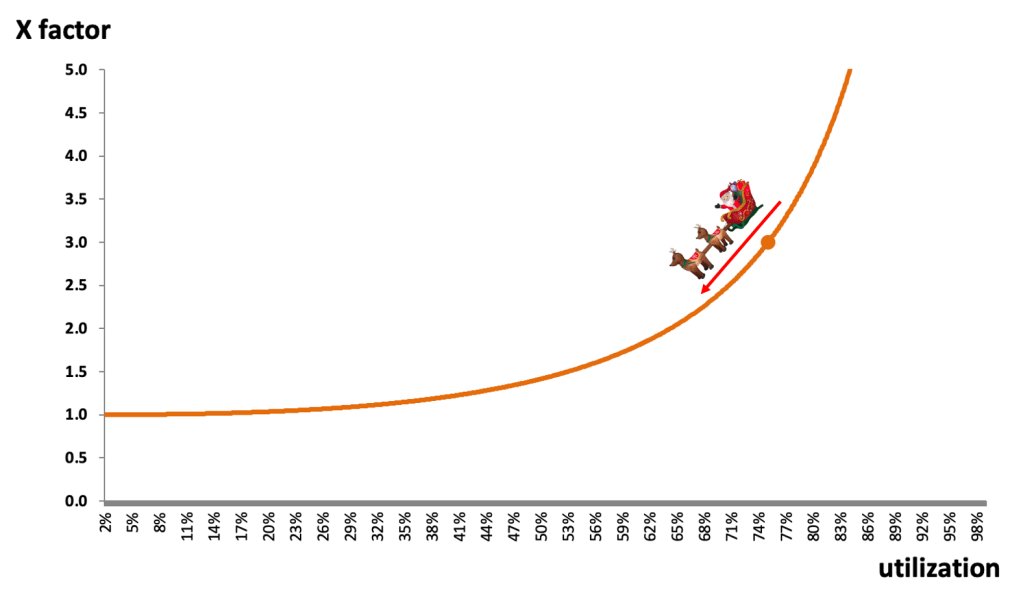
-
Equipment Uptime and FAB speed, part 3
My last post closed with a poll on achieved M-ratio values. Here are the results:

Unfortunately, not too many readers participated – so the statistics of the result are a bit weak. To some extend the data is reflecting my personal experience – what I have seen in various FABs. There is a significant amount of FABs (40% in the poll results) which have M-ratios below 1. In other words these FABs experience more unscheduled downtime than scheduled down time. The majority of the FABs in the poll (60%) shows a M-ratio greater 1 – they have more scheduled than unscheduled downtime.
Interestingly there are no M-ratios greater 5 looks like – which means at least 16.7% of all downtime is unscheduled. Compared to other industries this looks not too good. Imagine for example your car would have an M-ratio of only 5 …
Similar to semiconductor equipment, a car is nowadays a complex piece of machinery, but for sure there is not a lot of unscheduled downtime – at least not mission critical break downs.
With that in mind and knowing that cars of course have humans to transport and therefore the focus on safety and maintenance is (obviously) very different, I came up years ago with the picture below to define M-ratio classes for the semiconductor FAB world:
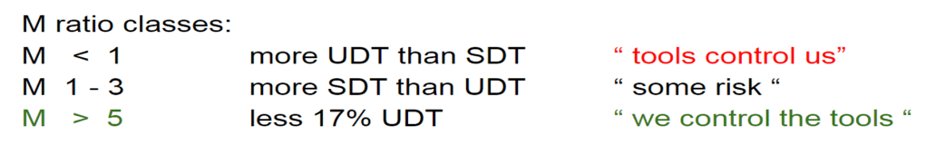
The reasons for having an M-ratio below 1 might be plentiful, but a key for that is for sure the general maintenance strategy of a FAB. M-ratios below 1 indicate in general a “run to fail” strategy. Often the reason for that is the cost aspect of a dedicated Preventive Maintenance set up, since man power, parts and meticulously executed scheduled maintenance are not easy and cheap to have. Another reason might be the age of the equipment and the availability of spare parts.
M-ratio as an indictor is not good for use as the one and only goal – since the real goal of equipment maintenance is to enable highest possible uptime – with “no-surprise” down times – but knowing the M-ratio of your factory might help to identify improvement opportunities.
Often the equipment organization in a FAB is measured (and valued) by indicators which only cover the pure equipment aspect. Therefore all optimization is focussed on getting these equipment centric indicators “look good”. Equipment performance and if an equipment goes down unplanned often can have massive impact on the WIP flow of the factory. Therefore the impact on the FAB cycle time and worst case on on-time delivery is not always taken into consideration.
In all my years I have seen a few typical “strategies” to deal with that problem:
- “run to fail” least cost maintenance approach (from a pure maintenance cost point of view)
- “zero unscheduled downtime” as an overarching end goal – to be fully in control, possibly even at the expense of lower overall uptime
- “predictive maintenance” do only interrupt when needed
While “run to fail” might be the easiest strategy to execute, it is also a completely reactive way of taking care of the equipment and often not good for the overall FAB performance. Aiming for almost no unscheduled downtime in the traditional way needs a very systematic and disciplined Preventive Maintenance program, which has been demonstrated to be doable but it comes at the expense of sometimes taking tools down for a scheduled maintenance, when it would be not really needed.
“Predictive Maintenance” seems to be the best solution of both worlds since it would only take an equipment down if it is really needed. The key here is to define “really needed” and to avoid running to fail. It would need to be detected early enough, so the needed action can be planned – for example “some time in the next few days” when it fits to the overall FAB and WIP situation.
I have seen papers and presentations about predictive maintenance for many years and it seems it was always the best thing to do.
The process and metrology equipment in a FAB represent a significant part of the total FAB investment and define to a large part what the overall FAB capacity and FAB speed will be. So one would assume that maintenance must have high priority, but M-ratio values in 2022 do not always support this assumption.
If you want to get more insight on the M-ratio indicator – a great read would be James P. Ignizio’s book

In chapter 8 of his book – titled
“Factory Performance Metrics: The Good, The Bad, and The Ugly”
M-ratio is discussed as well as other uptime related indicators.
-
Equipment Uptime and FAB speed, part 2
To illustrate which uptime pattern from the last post might be more favorable I will add some tool utilization to the same 3 charts:

the combined charts for the 3 scenarios are these:


This example assumes that the productive usage every single day is a flat 80% of the total time, which is a very optimistic assumption since in many factories with moderate to high product mix WIP arrival is highly variant for various reasons.
In my opinion: the tool group with less variability in the uptime pattern is in general a preferable situation – with one big exception: If all of the tool group downtime is scheduled downtime and therefore could be planned. The downtimes could be – at least in theory – perfectly synchronized to the WIP arrival patterns, which would reduce significantly the impact of downtime on the WIP flow and therefore also on the cycle time.
There is a very interesting indicator out there (that tries to measure exactly this) how much of the total downtime of a tool group is planned vs. how much is unplanned. It is actually a ratio:
M – Ratio ( or Maintenance ratio)

To calculate the M ratio of a tool group of interest – just sum up all scheduled down time hours and divide them by the unscheduled down time hours. The data collection timeframe needs to be big enough to capture all typical down events, so I recommend to use data at least from 3 months of history or more.
In the example above the result is 1 or in other words, this tool group has the same amount of scheduled or unscheduled down time. With respect to the synchronization to WIP arrival idea it would be of course good to have a better (higher M ratio). For example: a M ratio of 2 would indicate that only 33% of the downtime is unscheduled.
Before I dig deeper into the M ratio concept and how it can help I like to hear from the uptime experts out there: What are typical M ratio numbers you tool groups achieve ? Or should I ask : What M ratio numbers do your equipment teams achieve ?
Very curious to see the feedback. I will discuss the results in my next post
-
Equipment Uptime and FAB speed, part 1
I like to resume with the posts on the topic of FAB cycle time drivers. As mentioned in an earlier post – these are some of the key drivers for factory cycle time:
- overall factory size (number of equipment available to run a certain step)
- overall equipment uptime and uptime stability
- M-ratio
- rework rate
- product mix
- number and lengths of queue time restricted steps in the process flow
- lot hold rate and holt times
- degree of automation of material transport
- degree of optimization in the dispatching / scheduling solution
I covered the factory size topic already – so here are a few thoughts on equipment uptime. I think everybody knows and agrees that equipment uptime is a very key parameter. Equipment Uptime has direct implications on the factory capacity and even in the most simple, Excel based capacity planning model, you will find a column for planned equipment uptime. But of course the impact on capacity is only one aspect.
One could ask: Capacity – at what factory cycle time ? Based on the earlier discussed operating curve, a FAB has different capacity at different cycle times. Here comes the equipment capacity into the picture. The ideal FAB achieves the planned uptime on each tool group also in real life.
But what does it mean, if a tool group achieves its planned uptime ? We need to look a bit closer. Over what period of time does the tool group achieve for example 90% ? The capacity planners typically assume an average uptime number and somewhere in the fine-print you can find if this is meant to be for a 1 week, 4 weeks, 13 weeks or another time frame. For the real FAB these timeframes of interest are usually much shorter – if a few key tools are down right now for let’s say 2 hours – that might create already a lot of attention.
A deviation from the average planned uptime has the potential to impact the FABs cycle time. Assuming that the incoming WIP to a tool group is somewhat constant over time (which is already an optimistic assumption) higher or lower average uptime will result in higher or lower effective tool utilization and that means the wait time of lots will be different:
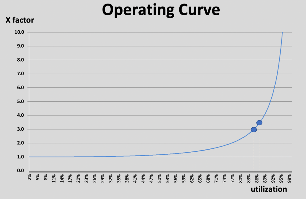
If we zoom in a bit more, tool groups with the same average uptime might have different impact on the lots wait time based on how the day to day, shift to shift or even hour to hour uptime looks like.
Below are 3 “constructed” uptime day to day cases to illustrate that.
Tool group A has every single day 10% downtime (red) and 90% uptime (yellow) – no big surprise that the average uptime is 90%
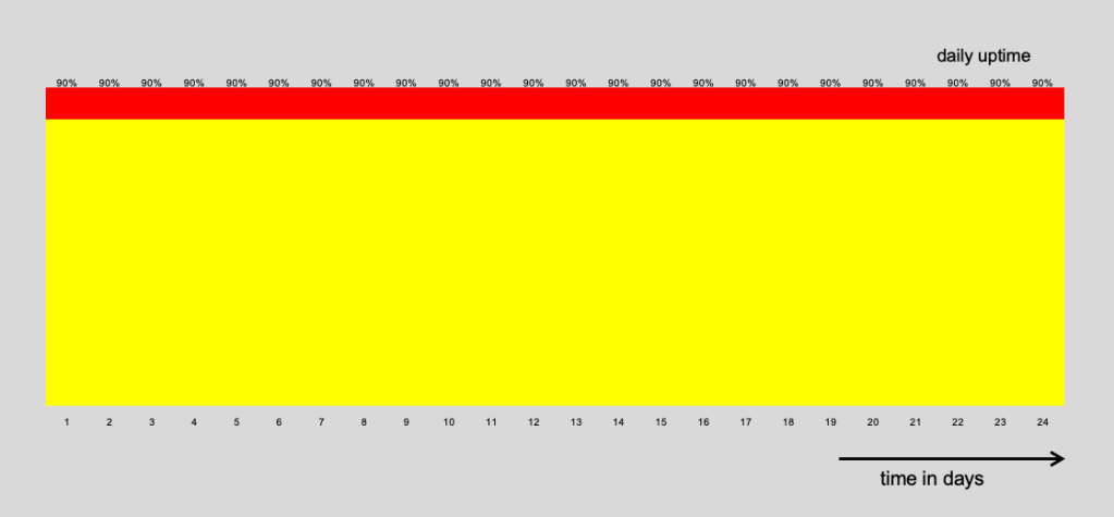
tool group A Tool group B has alternating days with 80% or 100% uptime – which will result in the same 90% average uptime for the full time frame
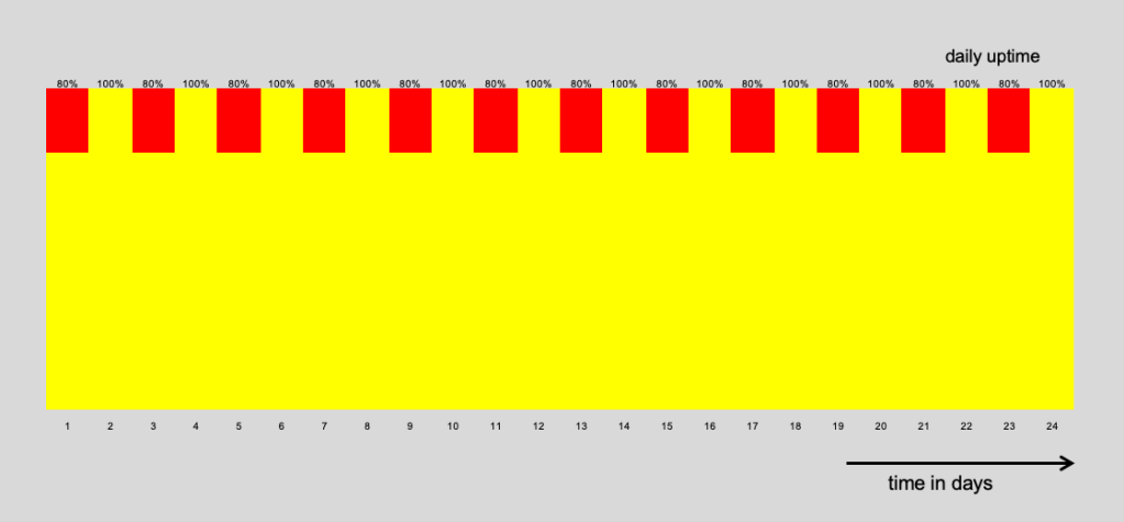
tool group B Tool group C has a very different down time pattern, but the average will be again 90%. To make you believe it – take visually all the red blocks more than 10% and fill them into the 100% uptime days and you get the picture from tool group A)
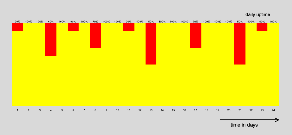
tool group C
If your capacity planning team is using average uptime values for capacity planning, these 3 tool groups are treated exactly the same. For static capacity planning purposes this will be fine, but if you like also to calculate/estimate/forecast the overall factory cycle time, these 3 tool groups will very likely impact the WIP flow differently and therefore the lot cycle time will be different as well.
Once this point of general understanding is reached the obvious next questions are:
1. Which uptime pattern is better for my factory A, B or C ?
(better as in: enables more stable and lower cycle time)
2. How do I change the not so good ones to look more like the best one ?I will discuss this a bit more in the next post.
-
Summertime (Blog) Blues
It has been a while, but summer in upstate NY is too beautiful to not enjoy it as much as possible. Downside is (at least for the blog) – I spend less time on the computer to write new posts.
So instead posting about Factory Physics and Automation topics, I do more of this:


Kayaking in the Adirondacks Later in fall there will be more time again for writing – for the time being just a very short post today.
There were 2 very nice articles written, referring to earlier posts from my blog and I think they are well worth the time reading:
Factory Size and how to benefit from it using advanced MES functionality – an article from Critical Manufacturing: LINK
Flexciton looks a bit more into the challenge of load port scheduling and load port utilization as a performance indicator: LINK
Enjoy the summer !
to get automatically notified about new posts:
-
19th Innovation Forum for Automation
Last week I had the honor to present a keynote at the 19th Innovation Forum for Automation in Dresden, Germany. After 2 years of virtual conferences, this year it was a full in person event again.
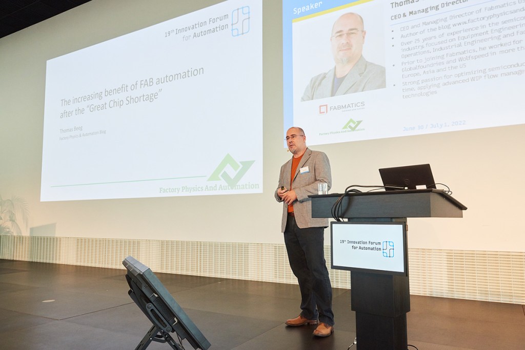
Here are the slides of my talk:
update: here are the video recordings of both days ( these are 3-5h videos):
-
Wafer FABs – how many are there ?
-
Fab cycle time and capacity planning
I did not discuss the results of the last poll yet. This post will focus on that.
Unfortunately, not a lot of readers did participate. The data is statistically more on the weak side, but I think the outcome is in line with what I was expecting:

It seems that 70% of the voters use a rather simple method to define the maximum allowed tool group utilization. This matches with what I have experienced in a lot of FABs.
Given the massive implications the FAB capacity profile has on the FAB cycle time it is surprising, that in todays heavily data driven world not more advanced methods are used. I wonder what is the reason for that ? Here is some speculation from my end:
- not enough resources to manage the significant amount of data
- input data quality for capacity planning is limited due to grouping of products and averaged assumptions
- real factory performance data is highly dynamic and hard to forecast for the next 2…3 months
- planning scenarios change so frequently, that a more detailed planning takes more time than the next scenario ask rolls in
- decision makers are used to simple rules like flat 85% – since they have worked for the last 20 years to some extend and more advanced methods are “black magic” and capital intense decisions will be not based on “black magic”
- FAB cycle time is more a high level target, the operations/engineering department needs to figure out in the daily business how to get the cycle time down
- or maybe the FABs which use more advanced methods simply did not vote here
I would love to hear feedback on these topics.
Leave a comment
Over the next weeks my posting activity will slow down a bit due to a lot of travel on my side. One special highlight is coming up with my visit in Dresden, Germany to participate at the

where I will have the honor to give a talk. Check it out here (LINK) and maybe we can meet in Dresden in person . After the event I will post the slides here.
-
US Semiconductor Ecosystem Outlook
I recently attended the Advanced Semiconductor Manufacturing Conference (ASMC) in Saratoga Springs, NY and listened to a very interesting presentation.
Bill Wiseman from McKinsey & Company spoke about the future of the US semiconductor ecosystem and a few fundamental challenges which will have significant impact.

Bill is a longterm insider of the semiconductor business and I got his permission to post his slide deck here:
-
View into a FAB
Happy Easter everybody !
Today only a very short post – since I’m discussing here normally how semiconductor FABs work in terms of cycle time and output, I thought why not have a quick look inside a FAB ?
This post was triggered by a recent YouTube post of an Intel FAB walk, which nicely explains how a modern FAB looks like. Please see below a few links to see inside a FAB:
Intel in Israel: LINK
Intel in US: LINK
Bosch in Germany: LINK
Micron in US: LINK
GlobalFoundries in Singapore: LINK
TSMC in Taiwan: LINK
Vishay (200mm) in Germany: LINK
Infineon (200mm) in Germany: LINK
Bosch (200mm) in Germany: LINK
-
Equipment load port utilization vs. FAB speed
I received and interesting comment to one of the older posts:
The topic is indeed very interesting. Most modern semiconductor processing equipment come with 4 load ports. Maine reason for that is to ensure the process chambers can be utilized as much as possible and do not have idle time because of exchange of lots. A simple 3 Chamber tool with 4 load ports might look like this:
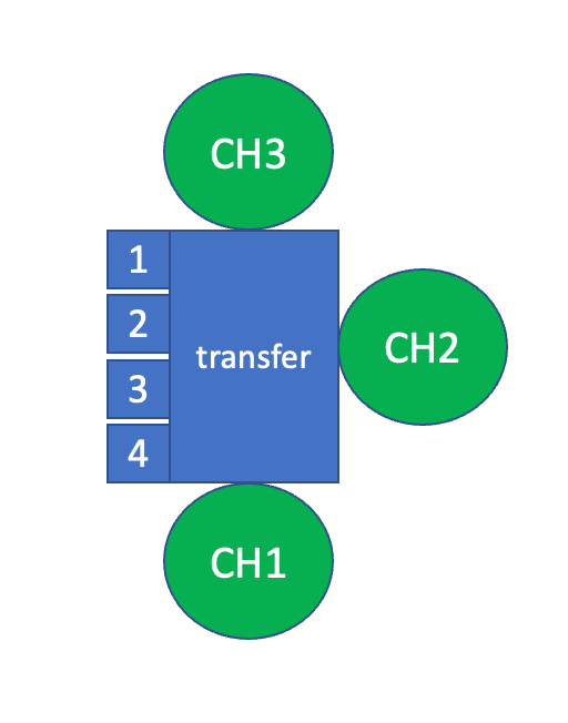
Individual wafers will be removed from the carrier on the load port and travel through the various equipment modules depending on the actual process recipe sequence. An example is shown below:

Let’s assume there are lots with 5 wafers processed on this tool. The wafer will sit in different chambers at different times. Below is a simplified example, which ignores the time a wafer spends in the transfer chamber for handling.
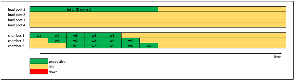
The reason why tools have more than 1 load port is illustrated in the picture below. For example: let’s assume load ports 2, 3 and 4 are down and only load port 1 can be used.
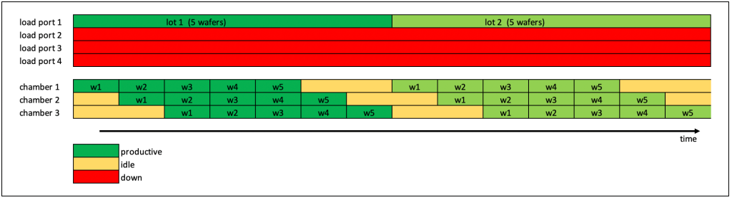
Lot 2 can only be loaded after lot 1 has finished and was unloaded from load port 1. This will lead to idle process chambers:
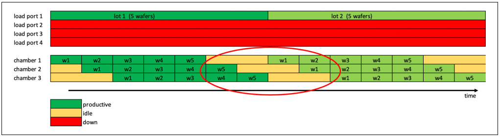
Having more than 1 load port available will allow to load the next, while the 1st lot is still processing and therefore these chamber idle times can be prevented, since the 1st wafer from lot 2 can be processed immediately after wafer 5 from lot 1:
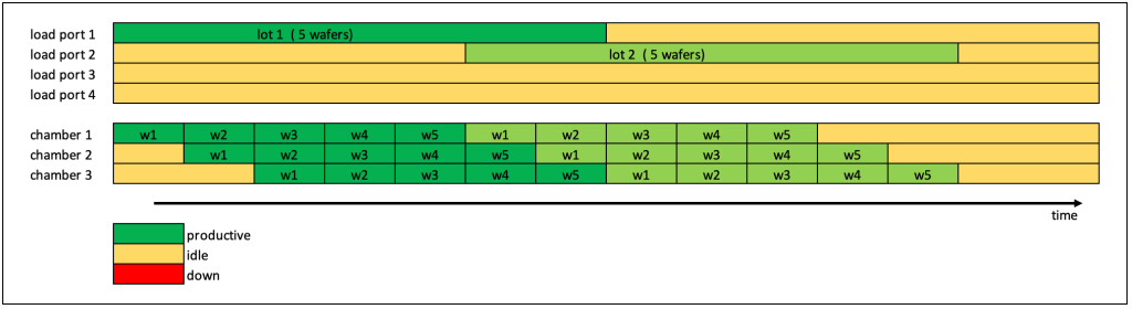
To load lot 3 early enough – to prevent chamber idle times between lot2 and lot 3 – load port 1 is again available:
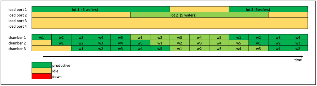
At least in the example above, 2 load ports would be more than enough to keep the process chambers busy all the time. Why do equipment vendors deliver most of the tools with 4 load ports ?
How many load ports are really needed depends on a lot of factors. In my basic example above I ignored most of them. As always the devil is in the detail, but here are some factors which influence the need for more load ports:
- number of process chambers on the tool
- process times of the individual chambers
- time a wafer spends for transfer between chambers
- wafer flow logic through the tool (serial, parallel)
- load port down times
In my experience most of the tools with lot processing times greater than 15 … 20 minutes can easily be fully utilized with 2 load ports, since there is enough time to transport the next lot to the tool, while the current lot is still processing.
But let’s go back to the comment which initiated this post:

I completely agree, that having always all load ports loaded will lead to higher wait times. Here is the theory behind that. To illustrate the effect I will use a simple FAB with 4 process steps, running on 4 different process tools. Each process tool has 4 load ports and the lot process time is 1h on each step. Lots have 25 wafers each:
In this scenario – with all 4 load ports always loaded – these would be the factory performance data:

Let’s look at a second scenario, which only has WIP on 2 of the 4 load ports:
Since there is now significantly less WIP in the factory, the overall factory cycle time is much faster – at the same FAB output:
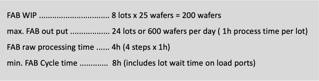
Here is my take on this: Having multiple load ports on a processing tool is for sure very beneficial since it will enable maximum possible equipment utilization. Having all tool load ports loaded with lots all the time is definitely in most cases not needed to achieve maximum factory output and clearly a sign of a relative slow factory. As a matter of fact, one can easily estimate the overall factory X factor by this logic:
Average number of lots waiting per tool equals the FAB X factor.
This ignores that lots might have different number of wafers and different processing times for different products at different steps, but if a FAB has always all 4 load ports on all tools loaded with lots and possibly 2 more lots waiting in stockers, this FAB will run not faster than an X factor of 6.
Another interesting fact is that there are a few tools (mostly with very fast processing times) where even 4 load ports are not enough to always feed the tools with wafers fast enough.
A last statement on the topic of load port utilization: I have seen in multiple cases that the manufacturing departments use load port utilization as a metric – mainly with the interpretation that idle load ports are “bad”.
I think this is driven by the general desire to have tools fully utilized and have enough WIP on the tool for the next hours, so even in case upstream tools have a problem or lot transportation is slow, the tool group of interest can still process “full steam”
-
Wafer FAB – size does matter !
In one of the earlier blog posts (LINK) I received interesting feedback on what are “acceptable” FAB cycle times. The results showed big differences and I think this is mainly based on voters professional experience. There are a lot of factors which influence a factories capability to achieve a certain cycle time. If we assume 2 factories are running the exact same technologies and process flows – but have different actual factory cycle times – the difference will not come from the process times of the lots, but mainly from different wait times. Key drivers for wait times are:
- overall factory size (number of equipment available to run a certain step)
- overall equipment uptime and uptime stability
- M-ratio
- rework rate
- product mix
- number and lengths of queue time restricted steps in the process flow
- lot hold rate and holt times
- degree of automation of material transport
- degree of optimization in the dispatching / scheduling solution
Let’s dig into a few of them in more detail.
Factory Size
One of the biggest drivers for factory cycle time is the size of the factory itself. The key reason for this is that processing equipment does not have 100% uptime. In a very simple way: If a factory would have only 1 equipment to process a certain step and the equipment is down there is no path for the lots and they have to wait until the equipment is back up. If there is more than 1 equipment available, lots have a path to progress and there will be less waiting time. This effect can be seen very well with the help of operating curves:
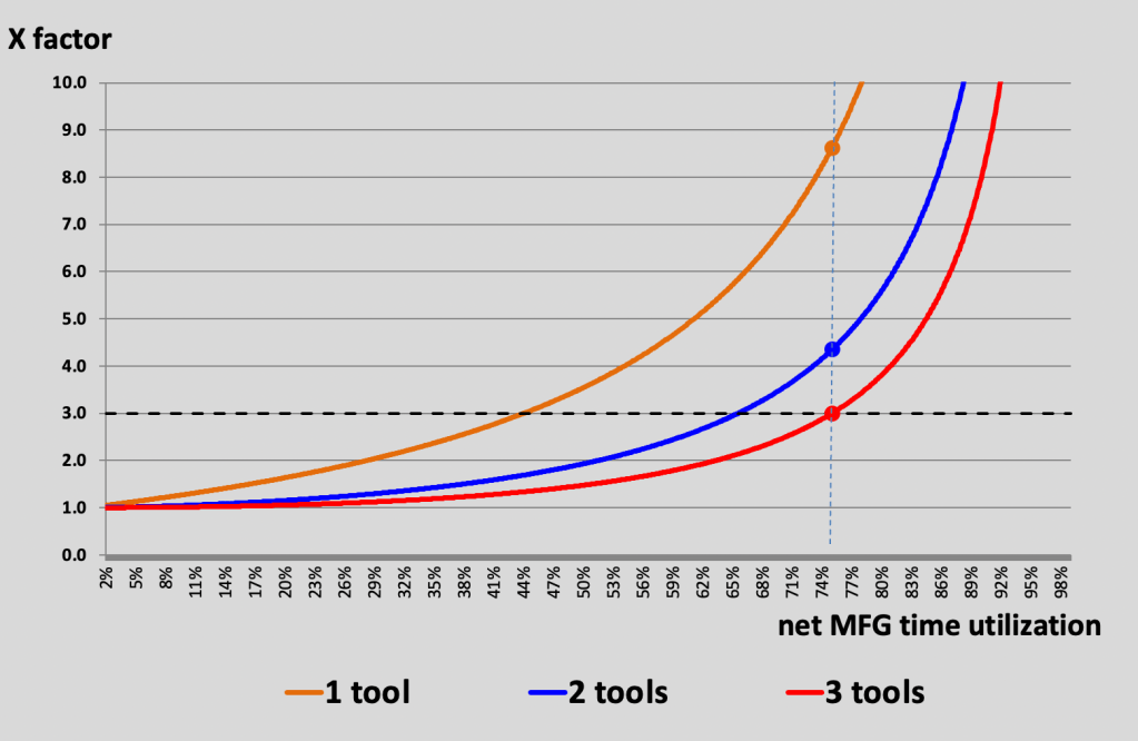
Having more than one tool available to run lots will massively reduce the average lot wait time, if all other parameters of the tools are the same. Everyone in manufacturing knows this effect and for that very reason avoids having these “one of a kind” situations.
It also can be seen, that the effect going from 2 to 3 tools is smaller than going from 1 to 2 tools. I think a golden rule in capacity planning for semiconductor FABs is: “… avoid one of a kind tools as much as possible – or plan with very low tool utilization for these situations …”
For example if there is no way around a one of a kind tool and you still need to achieve cycle times around a X-factor of 3 – in the given setting – the maximum allowed tool utilization would be 44% !

The real interesting thing here is that of course each tool set’s operating curve is shaped differently and in order to understand the impact on the total factory cycle time, one needs to know and understand the operating curves of all tool sets in the factory. A second aspect to keep in mind is: How many times will a lot come back to a tool set – since this has big impact on the factory cycle times as well.
Example: The operating curve shows a X factor of 3 and the processing time at the tool group is 1 hour, which means there will be 2 hours of average wait time for each lot. Here is the impact on the overall factory cycle time based on the numbers of passes (number of times this tool set in in the flow)

Look at the last column – the impact can be massive !
Having all these effects in mind, I think it is easy to feel “relatively safe” if a FAB has at least 3 or 4 tools available for each process step. In my opinion it is a much better situation than having 1 or 2 tools available, but often the “name plate capacity” number of tools available in a capacity planning model is one thing.
How many tools or chambers are really available (and not inhibited, temporary disqualified or for other reasons not used) is often a different picture. Also, based on my experience, typically the actual number of tools available on the floor is seldom bigger than in the capacity (and cycle time) planning model.
improvement potential: Frequently check the real available number of tools vs. your capacity plan !!!
Back to the statement “… having 3 or 4 tools available is relatively safe …” – the positive effect of having more tools is of course also there at greater number of tools. As in the picture below, a 4 tool tool set runs nicely at an X factor of 3, but look what happens to cycle time if we would have significant more tools:
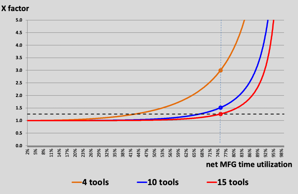
This is the real reason, why the big players in the semiconductor wafer FAB business build MEGA FABs. Having a very large number of tools in parallel allows to run at very fast FAB speeds and still utilize the expensive tools much higher. Now take into account that tool pricing also will be lower – if a FAB orders 10 tools instead of 2 or 3 – the whole thing becomes really desirable.
Of course, building a very large FAB requires a lot of upfront capital and also the expected demand needs to be big enough to fill a bigger FAB, but if you have the choice and are in doubt – always GO BIG, it will pay benefits for many years to come.
To close this post – I’m curious how the industry is dealing with the effects described above – specifically for planning purposes. In your capacity planning model: How do you define the maximum allowed tool utilization for a tool group ? I’m assuming that 100% planned utilization is not a legit assumption to avoid extremely high FAB cycle times. How is this modeled based on your experience ?
-
The value of 1 day of factory cycle time
Thank you everyone who participated in the last poll. Participation was significantly down beside the fact, that there were plenty of post viewers. My interpretation is that the readers are not too sure about the actual value of 1 day of cycle time. This observation is also in line with my personal experiences from working in semiconductor wafer FABs. It seems like that everybody acknowledges that fast cycle time is a good thing and it would be valuable to work on that – but what the actual value is – there is no clear understanding. The results of the poll itself look accordingly:

the same data sorted by the $ value:

The majority of voters pointed towards a few hundred thousand dollars but 33% said it is a million dollars or more !
I think one of the reasons why the real value of cycle time is not clearly defined is the missing of an accepted and standardized model how to calculate or at least how to estimate. I have seen a few different approaches from very simple to very complex – and what is worse – different models will generate different results, which does not really help to build confidence in the numbers.
One very simple model is the following:
If we look at our factory operating curve and assume we are running at our voters favorite operating point:800 wafer starts per day at a X factor of 3 (or 60 days cycle time)
we can extrapolate the value of 1 day of cycle time by the following logic:
- 800 wafer starts per = 800 x 365 = 292,000 wafers per year
- 292,000 wafers per year times $1,150 selling price = $335.8 million revenue
If we now use the factories operating curve and “look” to the left and right of the current operating point we can do a very simply estimation of the value of 1 day of cycle time:

Since the operating curve is non linear there is a difference if we look towards lower or higher utilization – but if we assume only small changes around the current point – we can ignore this.
Towards higher utilization:
plus 50 wafers starts will lead to 20 days more cycle time or in a simple ratio:
2.5 wafers per 1 days of cycle time.
2.5 wafers x 365 days x $1,150 = ~ $1 million revenueTowards lower utilization:
minus 100 wafers starts will lead to 20 days less cycle time or in a simple ratio:
5 wafers per 1 days of cycle time.
5 wafers x 365 days x $1,150 = ~ $2 million revenue
This is a big difference between the 2 numbers – but even if we use the smaller one to be on the safe side – $1 million is a serious number. Keep in mind, all the other benefits of faster cycle time are ignored in this simple model.
Another model – significantly more complex – which takes into account:
- revenue gain due to faster cycle time versus falling selling price
- revenue gain due to faster yield learning
It was developed by professor Robert Leachman. He teaches this method at the University of California, Berkeley. The complete coursework can be found here: LINK
I will not dig in more into the “fascinating world” of models to calculate the value of cycle time – instead will discuss a bit more the practical application of the value of speed.
Clearly the value of speed depends also on the overall market situation. In very high demand situation customers might be willing to tolerate higher cycle times, if they just can get enough supply. Factories tend to start more wafers in these conditions and simply “cash in”.
Still if the engineering team could implement measures to reduce the factory cycle time by lets say 1 day – management could “use” this gained 1 day of FAB capability to start a few more wafers – driving the FAB back to the previous speed, but deliver more wafers = more revenue.
In this scenario the question is:
1 day of cycle time is worth $1 million. How much will be the engineering team allowed to spent to enable this 1 day of cycle time reduction ?This comes down to how ROI is handled in the company – but there is a path to calculate this. It will enable dollar spending for cycle time and this is based on a model – which will support decision making – if a measure or change is worth implementing or not.
In my next post I will start discussing a few more details around the operating curve and most important – what can be done to improve.
-
Chip shortage and FAB performance, part 3
Today only a very short post !
Very interesting poll results ! Of course the poll left a lot of things open to free interpretation and assumptions, but as expected voters had different opinions. Here is the feedback chart:
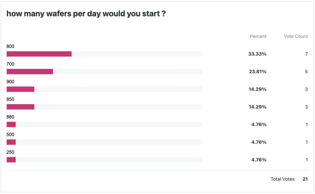
The same data in the context of the operation curve:
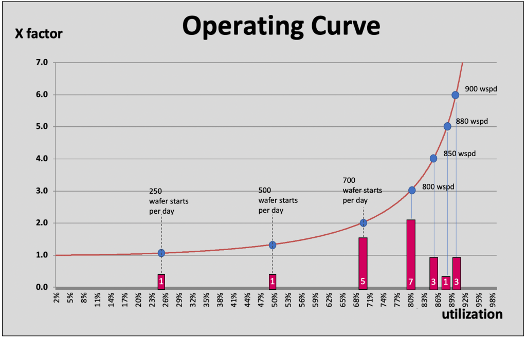
If I ignore the outliers at the 250 and 500 wafer starts per day mark the largest group of voters would trade
1 X factor of FAB speed for 100 additional wafer starts per day
and start 800 wafers per day instead of 700. Lets try to convert this into more understandable numbers:
1 X factor = 1 raw process time – for a “typical FAB” this could mean anything between 10-25 days of FAB cycle time. On the other hand, what do +100 wafer starts per day mean financially ?
Let’s assume there is an average profit of $150 per wafer – an additional 100 wafer start per day would add up to 100 x 365 = 36,500 more wafers per year or $5,475,000 more profit per year. This seems like an absolute no brainer.
How about an additional $5.5 Million dollar profit if we go to 900 wafer starts per day or $11 million additional profit ? Now the cycle time penalty looks very different. We would pay with 4 X factors or 40 – 80 days more FAB cycle time – still a no brainer ?
Here is a table for how this would look – assumption FAB raw process time = 20 days
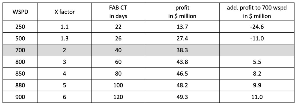
I think it comes down to the famous question:
What is the value of FAB cycle time – the value in $$ ?
Based on the table above it seems like shorter FAB cycle times are not really desirable, but at some point customers will turn away to order wafers from someone else – if lead times between order placement and actual wafer delivery are too long …
Experienced wafer FAB practitioners know that shorter overall factory cycle times can have a lot of positive effects:
- faster learning cycles to improve yield
- lower overall FAB WIP – lower overall inventory cost
- lower overall FAB WIP – lower risk of excursion impact
- faster detection of possible process issues
- faster reaction capability on demand / product mix changes
- likely better on-time delivery for low volume products
- …
The question really is: Until which point is it more beneficial to run the FAB faster (lower cycle time) since the benefits of being fast or outweighing the benefits of higher profit due to higher FAB output ?
I can not resist to put up another poll here to see, what the readers think is the value of 1 day of shorter (or longer) FAB cycle time. For our example factory above – running at these parameters:
- 800 wafer starts per day
- X factor of 3 or 60 days total FAB cycle time
- about 47,500 wafers of total FAB WIP
- 98% manufacturing yield (wafer scrap based yield)
- 90% die yield (electrical yield)
- cost per wafer of $1,000
- selling price per wafer of $1,150
- selling price more or less stable (chip shortage driven)
- high product mix in the FAB (greater 250 different products, running on more than 100 routes)
I can’t wait to see the results. To give a few more readers a chance to vote, I will keep this poll open for about 3 weeks – so the next post will be some time end of February.
-
Chip shortage and FAB performance, part 2
Reflecting on the wide spread of acceptable wait times and therefore acceptable FAB cycle times from the poll results, I was wondering: Why do people have these different opinions. I think it has to do with the actual factory conditions, the individual voters have experienced in their professional careers.
To have fast cycle times is an obvious goal, just how fast is “good” or possible ? The expectation must be influenced by real world experience, else everyone would have voted for the “less 30 minutes” bucket.
This leads to the question: Why do different FABs have different cycle times or different X factors ?
Absolute FAB cycle times are of course depending also on the raw processing times (RPT) of the products in the factory. For example:
RPT wait time cyle time X factor Factory 1 10 days 20 days 30 days 3 Factory 2 20 days 40 days 60 days 3 If just looked at the absolute cycle time – it seems that factory 2 is much slower, but in terms of how much wait time compared to the processing time (aka X factor) both factories perform similarly.
To really be able to “judge” or compare Fab speeds , cycle times or X factors need to be normalized to the overall factory loading or factory utilization. To explain why this is important I will use the picture of a 3 lane highway.
Imagine you use this highway for your daily commute to work and lets assume these basic data:
- distance from your home to work = 30 miles
- speed limit on the highway = 60 miles per hour
- you are not driving faster than the speed limit
- your “raw driving time” = “raw processing time” = 30 minutes
- the highway (the factory) is everyday the same, it has 3 lanes and a speed limit of 60 mph
Let’s try to answer this question: How long does it take to get to work?
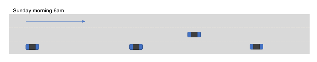
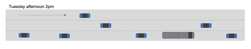

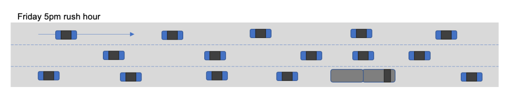
I think everybody will agree, that there will be very different driving times (cycle times) for the different days and times – all happening on the exact same highway (factory). The difference is the utilization of the highway. Now lets assume the same highway, but we throw in a lane closure – which actually means the highway has now reduced capacity:

The table below shows some assumed drive times (think cycle times):

The point of this example is, that the drive time on the highway is depended on how much the highway is utilized. Also important, the highway capacity has impact on the highway utilization and therefore on the drive time as well.
If we plot the data points in a chart it will look like this:
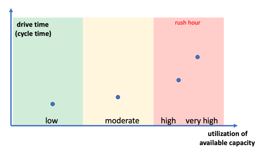
If we translate this picture into a semiconductor wafer FAB, there are a few interesting points to note:
- the FAB itself has a certain capacity
- the capacity of the FAB will not be stable if things like number tools, tool uptime or product mix change
- the utilization of the FAB is a result of a decision – how many wafers to start
- the very same factory can have completely different cycle times depending on the FAB utilization
I personally think this behavior, which is famously know as the operating curve, is one of the biggest challenges in the semiconductor manufacturing world (assuming that process stability and yields are under control )
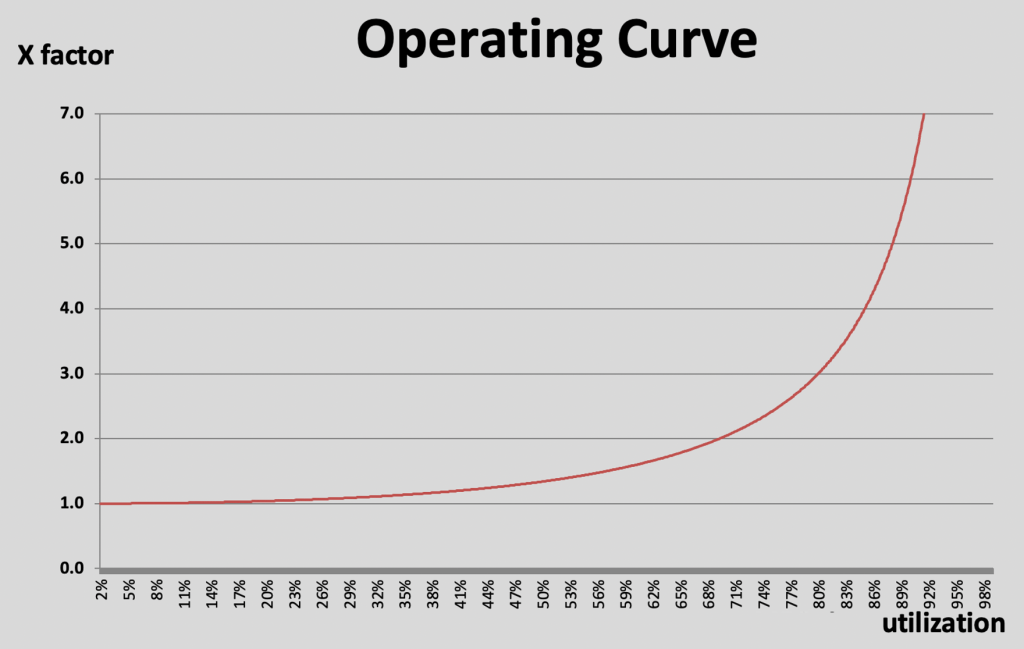
Each FAB has such a curve describing the factories ability in terms of what average cycle time can be achieved at which utilization level. Very important: the operating curve of different factories are extremely likely different (the shape of the curve)
The factory operations management team has “only” 3 tasks here:
- to know how the FABs operation curve looks like ( aka: what cycle time can be expected at which fab loading or utilization level)
- make a decision, how many wafers to start to achieve a desired cycle time and FAB output level
- execute daily operations and constantly improve the factories operating curve
To close today’s post, I like to ask again for your input. If you would be the FAB manager of the factory below, what would be your wafer starts decision – assuming you have enough orders to even start 1000 or more wafers per day ?

Results will be discussed in the next post.
-
Chip shortage and FAB performance, part 1
I like to be open – I could not resist to use the trendy “chip shortage” term to generate some interest. Everything I will discuss in this post series is of course fully applicable even in times without a chip shortage.
Let’s start with the results of my last poll:
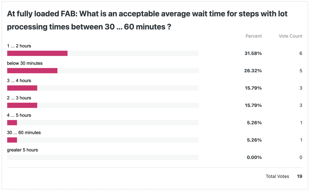
The spread of the answers is bigger than what I did expect to see, but it makes sense to some extent. Let’s chart the same data in a different way, sorted by the wait time buckets:

What this means is: For the same assumption on “fully loaded FAB” wait times between below 30 minutes and up to greater 4 hours are seen as acceptable. Let this sink in …
How does it impact FAB performance ? It will result in significant different total factory cycle times.
In order to illustrate that, let me put a few assumptions down to estimate what these wait times really mean:
- about 80% of all steps of a product flow typically fall into the category “processing time 30 – 60 min.”
- the remaining 20% of the steps are shorter or longer – let’s assume it will average out to 30- 60 min. as well
- for the estimation I set the 30 – 60 minutes range to a fixed 45 minute processing time
The cycle time of a single step in the product flow will be always calculated as (ignoring any lot on hold times):

Based on that we can easily calculate the cycle time of a step, given different wait times. For the wait times from my poll it would look like that:
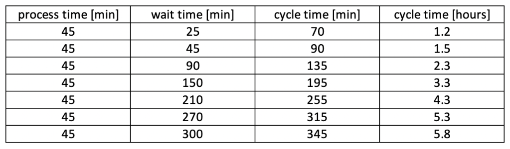
Another very common indicator to measure and compare cycle time is “X factor”.
Here is the definition of “X factor”:
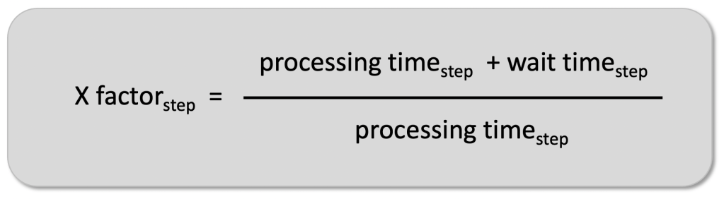
The same cycle timetable from above now including the X factor:
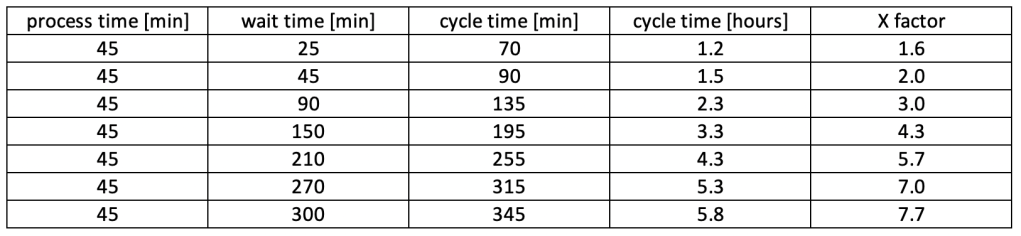
The true implication of the differences in what is an acceptable wait time comes to light if we scale this up to full factory level. For illustration purposes let’s assume the following FAB parameters:
- typical products have 40 mask layers
- average of 15 steps per mask layer or 40 x 15 = 600 steps in the flow
- basic assumption of 45 minutes average process time per step (as discussed above)
With these input parameters the total acceptable cycle time of this FAB would look like this:
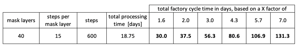
Different factories with different “acceptable wait time” assumption would have multiple months different cycle times for the same type of product.
I’m very sure, that FAB management with actual 80 days cycle time would really love to get down to 50 or 40 days – not to talk about 30 days. The magic question is: How ?
In my next post I will start looking into that.
-
Bottlenecks – download
here is the full bottleneck series as downloadable PDF file:
-
Bottlenecks, final part
Happy New Year !
This will be the last part of the Bottleneck discussion. As mentioned in part 3 – I think the most objective and telling indicator to see what is the true factory bottleneck is:
highest average lot wait time at a tool group
Wait time or cycle time in general is one of the very few indicators which can not be easily manipulated or “adjusted” by using different methods of calculation or aggregation. Time never stops and measuring the time between a lot arrives logically at a step and it starts processing at the step (on an equipment) are 2 simple time stamps which are typically recorded in the MES of the factory. For example:
lot arrived at the step: 01/02/21 4am
lot started processing: 01/02/21 10am
The wait time of the lot is super simple –> 6 hours.
The beauty of this metric is that no other information is needed – just these 2 time stamps. It will cover any possible reason why the lot waited 6hours – no matter what:
- equipment was not available due to down time
- equipment was not available since it was busy running another lot
- lot was not started due to missing recipe
- lot was not started due to no operator available
- lot was not started since operator chose to run another lot
- lot was not started due to too much WIP in time link zone
- lot was not started due to schedule had it planned starting at 10am
- lot was not started due to … “name your reason here”
One key part of the FAB Performance metrics – as discussed in part 2 – is:
- deliver enough wafers in time –> customer point of view –> cycle time of the FAB
In other words once the decision was made to start a lot into the factory it has some kind of target date/time by when this lot needs to be finished or shipped. Any wait time is by nature now a “not desired state” especially if the wait time is “very long”. That means tool groups which generate the highest average lot wait time will be very likely the biggest problem or bottleneck.
Let’s have a look at some example data to illustrate that:

The chart above shows the average lot wait times per step of our complete factory. Some steps have 1h wait time others have up to 6h.
Since this chart shows the data by step in the order of the route or flow it does not tell immediately which tool groups are the various steps running on.
The same data – including the tool group context – will tell this better:
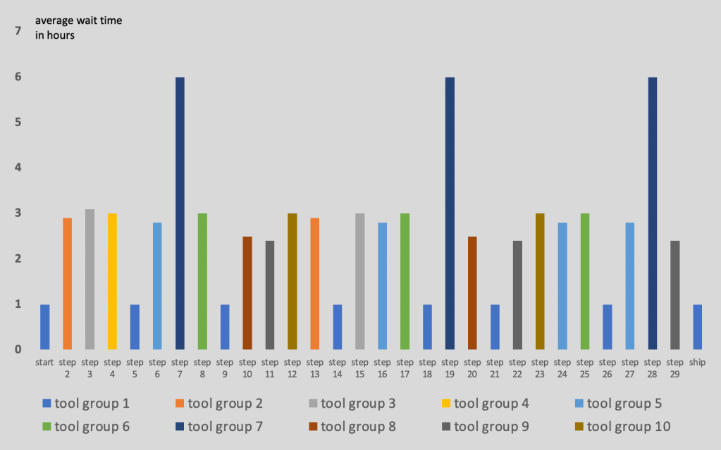
If we now aggregate and sort this by tool group instead of step we have our bottleneck chart:

From this chart tool group 7 clearly has the greatest average lot wait time of all tool groups. An interesting version of this chart is the “total wait time contribution” chart which shows the sum of the individual step wait times.
For example tool group 7 has 3 steps in the route and on average a lot waits on each step 6h. If we plot the same data as “total wait time contribution chart” we will not average the wait time of the individual step but add them: Tool group 7 will show 6h + 6h + 6h = 18h of total wait time for each lot.

Note that the sort order of the tool groups is now different. For example tool group 1 which on average has the lowest wait time (1h) is now ranked as number 4. From an overall “is this tool group a problem for the factory ?” point of view I say no – since lots barely waiting there – it just happens that tool group 1 has a lot of steps in the flow. I strongly lean to the average chart for the overall definition of the FAB bottleneck but recommend always to have a look on the cumulative chart as well.
In part 2 of the Bottleneck blog series I discussed the “Factory Utilization Profile chart”. I think this chart enhanced with the wait time data from above will give the “complete view” what is going on in the factory and will spark enough questions to dig in deeper at the right tool groups.
The chart below shows the data sorted by the highest average cycle time:

Obvious question is: Why is there so much wait time on tool group 7 at such low utilization or asked differently: half of the time the tool group is idle – why do lots wait on average for 6 hours ?
Or another one: How is tool group 1 able to achieve such low wait time ?
At this point I like to stop for a second and point you to an excellent source of additional discussion on the the topic of bottlenecks and cycle time:

FabTime Cycle Time Management Newsletter If you subscribe to the newsletter, you will have access to past editions as well !
Let me get back to the statement: Any wait time is by nature now a “not desired state” especially if the wait time is “very long”
Given the nature of the wafer FAB the ideal case of zero wait time at all steps is not very realistic since there are too many sources of variability in a factory. Therefore experienced capacity planners and production control engineers typically set an expected wait time target per step (and therefore by tool group). Using these expected wait times, the definition of “very long” becomes easier.
For example if
tool group A has an expected wait time of 2hours
tool group B has an expected wait time of 5hours
An actual achieved wait time of 6 hours would be kind of tolerable on tool group B but clearly seen as very high on tool group A.
Setting expected wait times per step and/or tool group depends on a lot of parameters, like:
- planned tool group utilization
- number of tools in the tool group
- duration of process time
- batch tool / batching time
- lot arrival time variability
- many others
I’m curious what the readers of this block think would be an acceptable average wait time for non bottleneck steps in a fully loaded factory.
Let’s assume that most steps in the factory have processing times of 30 – 60 minutes, running on non-batch tools, and the factory is fully loaded = the capacity planners tell you, you can not start more wafers. What would be an acceptable average lot wait time for these steps in your opinion ?
Please vote below, what you would see as good / o.k. / acceptable:
I will share and review the results in my next post.
-
Bottlenecks, part 3

Merry Christmas and Happy Holidays !
I hope everybody is having a good time with friends and family and after a lot of good food is ready sit down and discuss more details about factory bottlenecks. In today’s post I will start zooming in on the 3 not grayed out metrics from the poll results picture below:

To disclose my personal opinion upfront: I think that “highest average lot wait time” (or metrics that are derived from this) is the most objective way to measure and define what is the true factory bottleneck. But lets discuss all 3 of the metrics a bit.
highest miss of daily moves vs. target
I think every factory in the world is measuring and reporting in some way the number of “Moves” – the number of wafers which were processed/completed on a step in a day, a shift, an hour, for the whole FAB or departments and down to individual process flow steps and grouped by equipment or equipment groups.
“Moves” is a very attractive and popular metric for a lot of reasons:
- Moves can be easily measured and aggregated in all kind of reporting dimensions
- based on the numbers of steps in a process flow (route) it is clear, how many Moves a wafer needs to complete, to be ready to be shipped
- Moves is a somewhat intuitive metric – humans like to count
- target setting seems to be pretty straight forward – “more is better”
I personally think, measuring a FAB via “Moves” as the universal speedometer can be very mis-leading and might drive behaviors – which are actually counter productive – for the overall FAB performance. At the very least a well thought through and dynamic target setting is needed to steer a factory which is mainly measured by the number of Moves. The danger of Moves as the key metric might be less in fully automated factories, since the actual decision making is done by algorithms which usually incorporate a lot of other metrics and targets and therefore Moves are more an outcome of the applied logic, less an overarching input and driver.
In manually operated factories, where operators and technicians make the decisions, which lot to run next and on what equipment, a purely Moves driven mindset can do more harm then good – to the overall FAB performance.
I think a lot has been written and published on this topic and there are strong and different schools of thought out there, but I’m fully on board with James P. Ignizio’s view in his book
In chapter 8 of his book – titled
“Factory Performance Metrics: The Good, The Bad, and The Ugly”
“Moves” get a nice talk – in the “Bad and Ugly” department – for the very reason, that Moves can drive counter productive behavior. If you are interested in this topic – I strongly recommend reading the book.
Before I jump to the next metric – I just wanted to say – that I think that Moves are important to understand and is a useful indicator if used within the right context, but not “blindly” as the most important indicator, which drives all decision making.
highest amount of WIP behind a tool group
Almost one third of the voters picked this metric. Similar to Moves there are a lot of advantages to measure WIP:
- WIP can be easily measured and aggregated in all kind of reporting dimensions
- using “Little’s law” it is easy to define WIP targets
- WIP is a very intuitive metric, especially in manual factories – is my WIP shelf full or empty ?
In general – for daily operations – having a lot of WIP is seen as problematic, since it might lead to lots not moving, starvation of downstream steps and tools, long lot wait times before they can be processed. So high WIP is not a desirable status and very high WIP must be for sure a problem. I think here as well – it depends. For example it depends on what is the target WIP for the given context (like a tool group) to just try to lower the WIP as much as possible (“at all cost”) might lead to generating WIP waves in the factory and to underutilization and lost capacity.
Why do I not 100% subscribe to the highest WIP = the bottleneck ? It is simply, that the tool group with the highest WIP not necessarily has the worst impact on the FAB performance. Here are some data points for this:
Let’s assume we have a very small factory running a very short route – with only 30 steps. If we plot a chart showing the WIP (in lots) per step for each step and sort the steps in the order of the process flow – meaning lot start on the very left and lot ship on the very right – we get what is typically called a line profile chart.
In the picture below our factory is perfectly balanced ( if we define balanced as lots per step – another great topic to talk about) because on each step there are currently 3 lots waiting – or processing.

If we look a bit closer, different steps are of course processed on different tool groups, if we add this detail, the same factory profile looks like this:

For example tool group 2 has 2 steps in the flow and tool group 9 has 3 steps. Our bottleneck metric is the aggregation of the WIP by tool group (“highest WIP behind a tool group”). To find out, which tool group this is, we simply aggregate the same data from the line profile by tool group instead per step:

Tool group number 1 has the highest WIP of all tool groups in this FAB – it clearly must be the number 1 bottleneck – I do not think so. As discussed earlier, there is more content needed. For example, if tool group 1 is a scrubber process, which is typically in the flow a lot of times and it is an uncomplicated very fast process, having the overall highest number of lots there is not necessarily the biggest problem of the factory. Yes, one can argue, still it would be nice to have less WIP sitting at a scrubber tool set, but this is already part of the missing context, I mentioned earlier.
Measuring and reporting WIP is an absolute must in a semiconductor factory, but interpreting WIP levels and assigning them attributes like “high”, “normal” or “low” needs a very good reference or target value. Setting WIP targets should be done via math and science, to reflect what is the overall factory desired WIP distribution – in order to achieve the best possible FAB performance.
Before I close this topic for today – let me say: my simple “perfect balanced” line from the pictures above might not be balanced at all, if we incorporate things:
- different steps / different tool groups have very likely different capacities
- different raw processing times
- might be batch or single wafer tools
- might sit inside a nested time link (queue time) chain
- …
At this point I will pause and hope that I could stimulate some thinking and of course would love to hear feedback from the readers out there. The next post will be fully dedicated to the last open metric …
Thomas
-
Bottlenecks, part 2
A big thank you to everyone who voted in my little poll, here are the results:
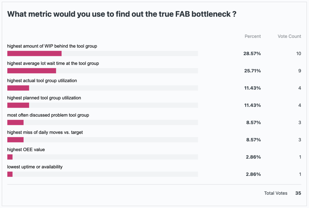
I kind of expected a picture like this – but what does this mean ? Here is my interpretation:
Bottlenecks are widely known as the one thing one should work on 1st to improve the overall FAB performance. But it seems we have different opinions how to measure and therefore to define what is the bottleneck.
For a real existing FAB, that would mean if different people or groups use a different definition, they would very likely identify different tool groups as the bottleneck – for the very same factory ! Of course we did not yet discuss what type of bottleneck we are talking about: a short term current one, a long term planned bottleneck or any other definition. Nevertheless people would identify very likely different tool groups as the key FAB problem …
Before we discuss this a bit more, I think we need to clarify what is the meaning of “bottleneck for the FAB”. In my opinion the purpose of a FAB is to make money and in order to do this wafers need to be delivered to customers in a way that the overall cost is lower than the selling price. Selling price also means one needs to have someone to sell them to – the CUSTOMER. For the purpose of this bottleneck discussion I exclude topics like yield and quality, assuming these are “o.k. and in control”. I will just focus on the 2 other key metrics for “FAB performance”:
- deliver enough wafers in time –> customer point of view –> cycle time of the FAB
- manufacture enough wafers –> total cost / manufactured wafers –> cost per wafer –> FAB output
So in my opinion, a bottleneck is a tool or tool group which negatively impacts the cycle time of the FAB and therefore the FAB output in general, but more specific the output of the right wafers (products) for the right customers at the right time (aka on-time delivery)
With that in mind, I think we need to define the metric in a way that it measures the impact to these 2 parameters. In a semiconductor FAB the typical unit to track wafer progress through the line is a “lot”. Hence, in order to measure how good or bad a tool group impacts the flow of lots through the line, we need to look a lot related indicator. This disqualifies grey marked ones in the picture below and leaves us withe 3 potential candidates

Let’s have a look at the greyed out metrics.
highest planned tool group utilization
It is very tempting to pick this metric since very high tool utilization signals to some extend, we might reach capacity limits soon. Also it is widely known, that tool groups with high utilization tend to also generate high cycle times. So there is a good chance, that the true FAB bottleneck has a high or the highest utilization – but there is not guarantee – that this is the case. This very much depends also on the overall utilization profile of the factory.
Another interesting topic to discuss in a future post is: What means “high” utilization and “high” cycle time? Similar, how to define “FAB capacity”, which I will discuss also in a later post.
highest actual tool group utilization
Everything I wrote above for the planned high utilization is valid for the actual utilization as well. I just like to add at this point, comparing actual tool group utilization and planned tool group utilization should be a frequent routine, to understand how close or distant the capacity model is able to follow the actual FAB performance – or should I say the the actual FAB is able to follow the capacity model ? You guessed it, an interesting topic for another post …
Before we move on into the next metrics, I like to spend a few thoughts on the topic factory utilization profile. The factory utilization profile is a chart of all tool groups, showing their average utilization ( planned or actual, for selected time frame, like last 4 weeks or last 8 weeks) and the tool groups are sorted in a way, that the tool group with the highest utilization is on the left and the one with the lowest utilization is on the right. A theoretical example is shown below:
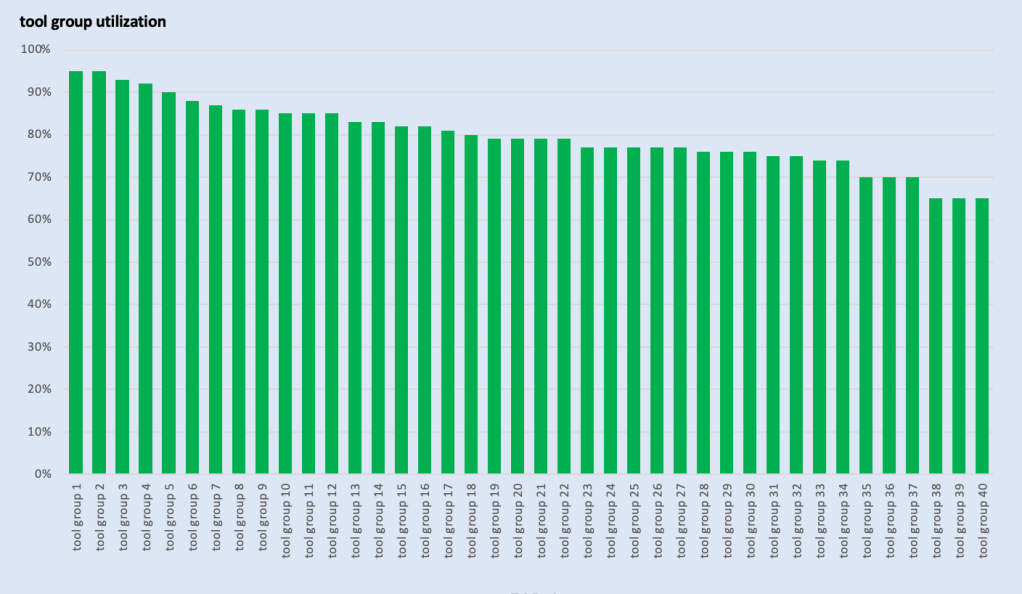
Different factories will have different utilization profiles. Even the very same factory will have different utilization profiles over time if things like wafer starts, product mix, uptime or cycle time change. So I always thought it is a very good idea, to keep an eye on that and also compare the profile planned data vs. actual data. An example of comparison (with dummy data) is below.
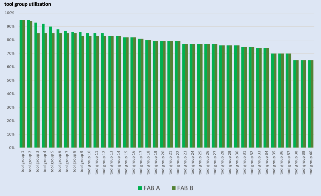
For example: Look at tool group number 3 ! How likely will become #3 a problem in FAB A vs. in FAB B ?
I think you get the general idea, but there is much more interesting stuff to read out of FAB utilization profiles. Before we go there – have you lately checked / seen your FABs utilization profile ?
most often discussed tool group
This metric has some advantage, since it is not focusing on one specific indicator and if a tool groups is very often in focus, it has for sure some problematic impact on the overall line performance. I rather would choose real data based metric, but for FABs with less developed automatic data generation and data analytics capabilities it is a usable starting point. I also like about this approach – once used for some time – it will inherently drive the demand for a more data based approach – to find out, why is a tool group discussed so often and where to start with improvement activities – which in today’s manufacturing world is an absolute must in my opinion.
highest OEE value
OEE it feels had its peek time when a lot of people talked about it, but it seems lately the topic became a bit quieter. The OEE method itself has its value, if used on the right tool groups with the right intentions. If applied solely to increase the name plate OEE value of every tool group in the FAB, it can become quickly counter productive and hinder the overall FAB performance ( at least if FAB performance is defined and measured as proposed in this post) In my active days as an FAB Industrial Engineer I often used the slogan:
“… if the OEE method is used the right way, its target should be not to increase the OEE value of the tool group, but increase the tool groups idle time …”
If OEE projects are aiming in that direction, they will for sure help to improve the overall FAB performance, but as the key metric to identify the biggest bottleneck I would not recommend to use OEE.
lowest uptime or availability
As mentioned above, uptime is a tool or tool group focused metric and for sure a very important one in every FAB. While low uptime is absolutely not desirable, it is not a good indicator if the tool group is indeed a factory bottleneck, since it will not tell us anything about the actual impact on the FAB without other information.
At this point I will stop for today. In my next post I will spend a bit more time on the 3 remaining – lot related – indicators and will also share, which one I think will be the most useful one to use. As always, I would love to hear feedback from you via a comment. One last thing: I will eventually stop announcing every new post via LinkedIn, so if you want to get notified when there is new content here, please use the email subscription form below
Happy Holidays !
Thomas
-
Bottlenecks, part 1
Almost 15 years ago I had the opportunity to attend a 4 day seminar with the authors of the well known book “Factory Physics” LINK

In the opening session we talked about what is limiting factory performance and sure enough bottlenecks came up. The question was asked , what can be done to improve a bottleneck. After a lively discussion between all attendees about what they have done or what they think should be done, Dr. Mark Spearman stated:
“… I propose you walk on the factory floor and look at the tool or tool group and see if it is indeed running (at full speed and efficiency) …”
I had a pretty big “aha !” moment and I remember this, like it was yesterday. But this proposal comes with another interesting challenge:
How do we know what is the factory bottleneck ???
I think to answer this question correctly is the foundation for a lot of things. In its simplest form, the correct answer would lead the folks who actually want to see the bottleneck on the floor to walk to the right tool/tool group. Obviously, there is much more connected to that, for example:
- where to spend resources for improvement activities
- if the bottleneck capacity is used to define the overall FAB capacity, it would be great, if the correct tool/tool group was identified
- where to spend capital to buy another tool
How do we find out, what is the factory bottleneck tool group ? One obvious answer is lets look into data – what data – and how do we know it is indeed the bottleneck. The answer becomes quickly ” … it depends …”
It depends on what is the definition metric and I have seen a few of them so far:
- highest tool utilization as per capacity planning numbers
- highest tool utilization as per actual numbers (daily, last week , 4 weeks ?)
- highest amount of WIP behind tool group
- highest average lot wait time at the tool group
- highest miss of daily moves vs. target
- frequency / intensity a tool group is discussed in morning meeting as a “problem kid”
- lowest tool group uptime ( or availability)
- highest OEE value
I’m pretty sure all of these metrics have some value, if used in the right context. I do have my own opinion, what I would select as the key metric, to declare the FAB bottleneck, but I really like to get some discussion going here, therefore I like to run a little poll, to see what the majority would select as the key metric:
I can’t wait to see the results. I’m fully aware that the answer selection is not that straightforward without more content – so if you like to provide thoughts, please use the comment functionally at the bottom.
I will share and discuss the results in my next post, sometime before the holidays
Thomas
-
Hello
Hello everybody,
I finally decided to start my own blog. It will be all about – surprise –
Factory Physics and Factory Automation
Why am I doing this ?
Over the years I had the chance to work very closely in different companies and their semiconductor factories and I found that especially in the non leading edge companies/FABs a lot of folks are very interested in these topics – but often even basic principles are not known or understood. This was often true for all levels throughout the organization, from operators up to the senior level leadership.
Throughout my professional career I enjoyed learning about these principles and using them for active decision making. I also realized that I liked sharing thoughts about those principles.
To keep this going also in the future, I will start in a loose frequency posting topics, questions and more. I hope you will get something out of it for your daily business and also contribute to a fruitful discussion and exchange.
Stay tuned for more and if you have suggestions for topics, please let me know, I will for sure give them a try.
Thomas
enter your email address and click subscribe:
Factory Physics and Automation blog
to share and discuss experiences in the field of semiconductor manufacturing operations and automation


Leave a comment