
In the last few weeks I had the opportunity to visit a few of our (FABMATICS) customer FAB’s here in the US – sure enough the topic of test wafers and the options and benefits to automate test wafer handling came up in all of them.
They all categorized themselves into the area of higher test wafer to product wafer ratios ( see the 1st post of the test wafer series) and mentioned they feel they have way to many test wafers in the FAB. Most of them also talked about challenges in getting tool time on process equipments to build new or recycle used test wafers.
From my own experience this is very common in less automated FAB’s where a lot of day to day decisions are still made by humans – who are often measured by daily or hourly production wafer moves.
To get a good control over the huge number of test wafers and the high number of different test wafer products one key starting point is to have transparency about test wafer WIP levels, use rates and who owns which test wafer.
I think to have a chance to be successful the general FAB mindset needs to be that test wafers have the same importance as production or engineering wafers.
This means that test wafers are completely modeled and tracked in the FAB’s MES system and test wafer lots are “running” on test wafer routes or flows – exactly like production wafers. This will not only enable real time monitoring of the test wafer status, but also opens up the capability to schedule and dispatch test wafers automatically using the FAB’s scheduling systems.
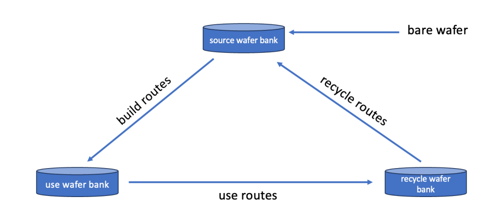
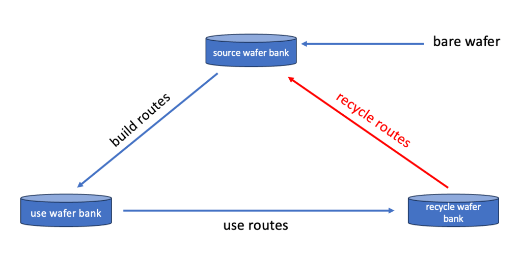
Test wafer Modeling
There are many ways of modeling test wafers, but one successful way of doing this is to follow the general life cycle of test wafers. A typical one would look like this:
- newly bought bare wafer
- built desired test wafer type
- use test wafer
- recycle test wafer
- scrap test wafer (end of life)
A graphical representation of such a cycle would be this:
Lets walk through the cycle on an hypothetical example for the following case:
After a maintenance event on a dry etch tool there needs to run a particle test wafer as well as an etch rate test wafer to confirm the the chamber is in spec for release to production. In order to so they need to be ready for use when the maintenance work is done.
Lets assume:
1. the particle test wafer needs to be of a certain cleanliness before it is used on the etch chamber
2. the etch rate wafer needs to have a known thickness of a certain film
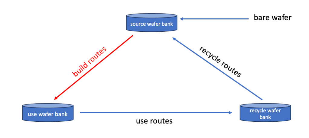
Build routes
to prepare or “build” these wafers the following 2 routes might be used:
Particle wafer route:
10 – start wafer from source wafer bank
20 – clean wafer at wet clean tool
30 – measure particles at metrology tool
40 – grade wafer – if below needed particle count -> o.k. to use
50 – store wafer in use wafer bank
Etch rate test wafer route:
10 – start wafer from source wafer bank
20 – clean wafer at wet clean tool
30 – measure particles at metrology tool and if good:
40 – deposit needed film on wafer at deposition tool
50 – measure film thickness
60 – grade film thickness – if good:
70 – store wafer in use wafer bank
Since it takes time to “build” these wafers it is clear that this has be done in advance of the actual use else their is high risk that the test wafers are not ready in time.
Another aspect of the build process is that of course not a single wafer will be build, but instead full lots (like 25 wafers per carrier).
This also means in the use bank there are likely multiple ready to use wafers sitting in the same carrier.
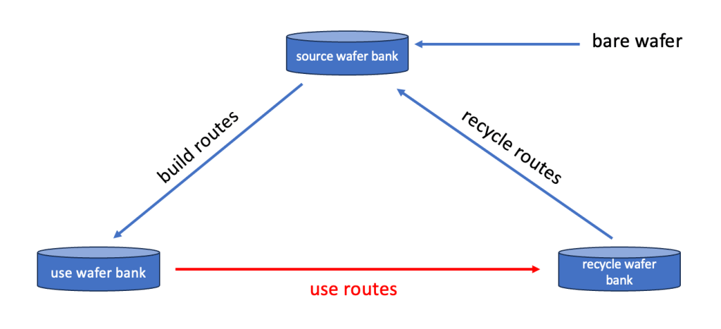
Use routes
To be able to actually “use” the 2 wafers for our post maintenance check, again a couple of things need to happen, which is typically managed by using “use routes” examples for or 2 wafers could be:
Particle Test wafer
10 – start wafer from use wafer bank
20 – split out 1 wafer into an empty new carrier
30 – run (cycle) wafer through the etch chamber
40 – measure particles added by the etch tool
50 – if particle adders are in spec – set flag in MES to “good to use in production”
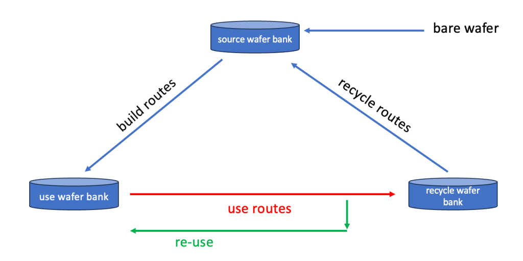
60 – grade wafer – if still good for next use – send back to use bank, else
70 – store in recycle wafer bank
Etch rate test wafer
10 – start wafer from use wafer bank
20 – split out 1 wafer into an empty new carrier
30 – run etch rate recipe at the etch chamber
40 – measure new film thickness at thickness measurement tool
50 – if etch rate is in spec – set flag in MES to “good to use in production”
60 – grade wafer – if still good for next use – send back to use bank, else
70 – store in recycle wafer bank
based on the option of directly re-using an already build and used wafer the model becomes this:
Recycle routes
Lastly, but also very important – what to do with all the used wafers ?
For cost saving reasons most FAB’s have implemented in-house recycling flows to “clean” the used wafers and put them back as “like new bare” wafers in the source wafer bank
For our 2 wafers (very likely in one lot/carrier together with other similarly used wafers sitting in the recycle bank) these routes could look like this:
used particle test wafer:
10 – start lot from recycle wafer bank
20 – clean wafer at wet clean tool
30 – measure particles at metrology tool
40 – grade wafer – if below needed particle count -> o.k. to use as “like new”
50 – store wafer in source wafer bank
used etch rate test wafer:
10 – start lot from recycle wafer bank
20 – completely etch all remaining film from wafers at etch tool
30 – measure film thickness ( should be zero now)
40 – measure particles and if good
50 – store wafer in source wafer bank
These examples of routes are of course extremely simplified. I conveniently ignored to describe all the needed lot ID and product ID changes which are involved in this life cycle, but it should be good enough to illustrate the principle.
A key part of the test wafer process is the frequent change of wafers into different carriers. Typically these happen at least at the read marked “points” in the flow:
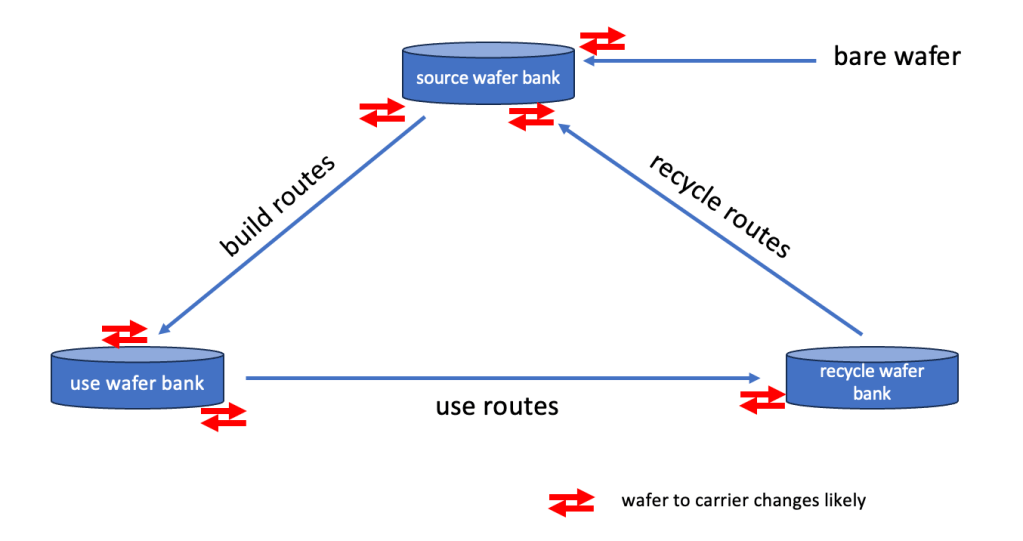
Depending on how automated a FAB is this can be a massive effort and drives a lot of operator time. Therefore the test wafer process it is a prime target for automation efforts.
Final thoughts
There are many more aspects of how to model and run test wafers in a FAB, which all have their pros and cons as well as depend on general policies the FAB applies: A few of the more interesting ones are:
- Do the FAB policies and CIM system capabilities allow multiple different lots to be stored and transported in the same carrier ?
- How is test wafer ownership organized ? For example: do different areas manage their own test wafers or is it allowed to share for example particle test wafers with other areas ?
Depending on how this is organized it might reduce the overall amount of test wafers – or not. - How are minimum and maximum stock levels at the 3 wafer banks defined ?
- How and where are test wafer lots stored and tracked from a physical location point of view ?
“somewhere in one of the 3 shelves over there” vs. in a stocker – makes a big difference - Do FAB policies require fresh pre-measurement data before each use or can old post measure data be used to save time. And if yes, how old can the data be ?
- How often can wafers be recycled before they are not usable anymore ?
- What is the scheduling/dispatching logic for test wafers on build and recycle routes at process tools which also run production lots ?
- Is there regular test wafer WIP level and test wafer aging reporting set up ?
- Who owns the test wafer “business” in general ? Operations ? Engineering ?
- Are there dedicated engineers assigned to manage test wafers in the FAB ?
- What happens if a test wafer in use case comes back with data out of spec ?
Is it a simply re-do of the test wafer run – and if yes – is it automatically a second run ? - How many of the traditionally on test wafers done tasks can be done directly on product wafers (at what risk) to save test wafers altogether ?
- Is there data available on how often process equipment has extended down time due to no test wafers ready ?
- Which of the test wafer uses cases are “gating” – meaning the process tool tested has to wait until post measurement data is available ?
- What is the frequency of scheduled test wafer runs? daily, weekly, every 10 days …
- How advanced is the deployment of run to run controllers to avoid seasoning, warm up or send ahead wafers ?
I’m sure I missing a lot more aspects. One thing is clear, test wafers have a huge impact in a FAB – and based on everything written above this is not a small “Friday afternoon” task.
To manage this “zoo” successfully:
1. test wafers need to have the same importance as any other wafer in the FAB
2. a well defined set up in MES is needed
2. ownership needs to be defined
3. engineers need to be allocated / dedicated
4. automating the kitting, de-kitting as well as the transport of test wafer carriers will significantly improve efficiency (spoiler alert: Fabmatics’ TESTWAFERCENTER can help with exactly that)
Happy Test Wafering 😉


It’s great to see such detailed information about their importance in semiconductor manufacturing. Your explanation of their role in quality assurance and cost efficiency is particularly helpful. Keep up the great work in sharing valuable industry knowledge!
LikeLike
“A comprehensive and insightful deep dive into the complexities of test wafer management in semiconductor fabs! Managing test wafers with the same priority as production wafers, optimizing MES setups, and automating handling processes are crucial steps for efficiency and cost reduction. The level of detail in this discussion highlights how automation can significantly improve test wafer workflows. Great read!
LikeLiked by 1 person
thank you for the nice feedback !
LikeLike