
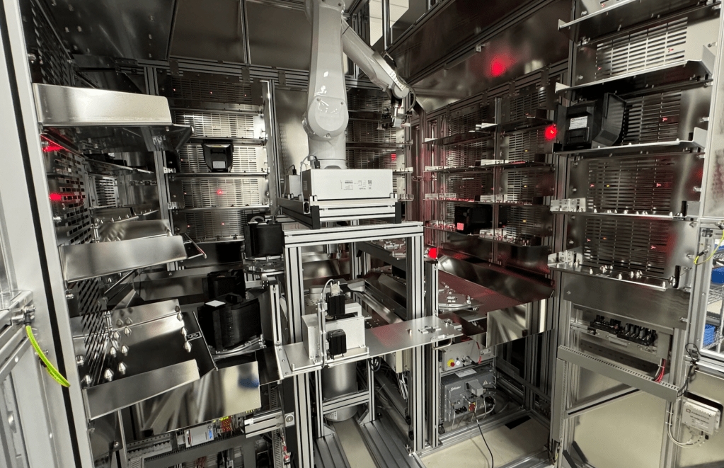
Inspired by the recent LinkedIn post from Fabmatics about the TestWaferCenter (LINK)
I thought it is time to look a bit closer at the general topic of “test wafers”. So what are test wafers ?
To keep it simple I will use the term “test wafer” for any non-product wafer in a FAB. Test wafers are the unsung hero in every FAB – almost like electricity and water in your home – you really only notice them when they are not available. Typical variants of non-product or “test wafers” are:
- wafers to qualify / re-qualify a process equipment after a maintenance event like thickness, etch rate or particle measurement wafers
- conditioning wafers, used to ensure process conditions in an equipment are ready to run product wafers, for example after longer idle times or recipe changes
- filler wafers typically used in batch furnace equipment to fill up empty wafer slots in the process boats
- monitor wafers – which are processed in parallel to product wafers in an process equipment to measure certain process results
- mechanical handling wafers used to teach / re-teach robots and general wafer handling inside of process equipment
- calibration “golden” wafers used to re-calibrate metrology equipment
In contrast to these wafers there are of course the product wafers, which are the wafers most people care about in a FAB:
- regular product wafers ( will contain at the end of the process real chips)
- R&D wafers – future product wafers ( will contain at the end of the process real chips)
- short loop wafers – to experiment and learn at certain segments of a real product process flow
The interesting thing about test wafers: these have massive impact on the overall FAB productivity:
a) in a positive way – by being always available when needed
b) in a negative way – by being not available when needed – for example after maintenance of a process equipment – missing qualification wafers will extend the equipment down time and therefore reduce the FABs capacity
In one of my past roles at a wafer FAB – every once in a while in the morning meeting we had reports about process equipment being extended down, since the needed test wafers were not available (in time) – obviously not a good situation to be in.
The fix to this situation seems easy – have the test wafers ready … ?!
But what does this mean exactly and how to make sure that this indeed works as desired ?
Unfortunately, the topic is very complex and it starts with the typically very large amount of different types of needed test wafers. The challenge is not only to have “a test wafer” available when needed, but the “right” one. To ensure the availability of all needed types of test wafers, FABs will have stock levels of these wafers and if summed up it can add up to impressive overall numbers of test wafers in a FAB.
One useful indicator on how complex the test wafer topic in a FAB is, is the ratio between product wafers and test wafers.
For example:
if a FAB has a total product WIP of – let’s say – 100,000 wafers and in parallel has also about 20,000 test wafers “sitting” in the FAB the ratio would be 100,000 : 20,000 or 1 : 0.2
if a FAB has a total product WIP of 100,000 wafers and in parallel has also about 100,000 test wafers “sitting” in the FAB the ration would be 100,000 : 100,000 or 1 : 1
In my 29 years in semiconductor I have seen vastly different product to test wafer ratios and I’m super curious what the situation looks like nowadays. The need for test wafers also is a function of the criticality of the process nodes running in a FAB. For that reason I divided the poll below into 2 groups:
- 300mm FAB – assuming that these mostly run more advanced process nodes
- 150 and 200mm FAB – typically running more mature and legacy process nodes
If you are working in a 300mm FAB:
Similarly, if you are working in a 150mm or 200mm FAB:
I will share the results of these pools in my next blog post – very much looking forward to see the numbers !
Test wafer management does come with one other challenge: low number of wafers in a carrier.
No matter which carrier type your FAB uses:
- 300mm FOUP
- 200mm SMIF pod with a cassette inside
- 150mm or 200mm box with a cassette inside
- 150mm or 200mm open cassette
Typically product wafer carriers contain more or less close to 25 wafers per carrier, while test wafer carrier very often do only have 1, 2 or 3 wafers inside.
It means that often a surprising large amount of carriers is occupied by test wafers and that requires a very controlled carrier management to not run out of available empty carriers (and storage places). I’m curious here as well, what is the overall situation nowadays in the FABs ?
If your are working in a 300mm FAB:
Similarly, for a 150mm or 200mm FAB:
Please provide some feedback using the polls if you have the needed data available. It will help to focus in my next blog post on the right topics.
If your not subscribed to my blog yet :

As is often the case, we are thinking about the same thing at the same time. My newsletter tomorrow will have a subscriber question on this topic. Your post was just in time for me to add a link. — Jennifer
LikeLike
haha – interesting, thank you for adding the link, looking forward to the newsletter !
LikeLike